TSMC’s Advanced Packaging Capacity
TSMC’s CoWoS capacity is in the focus after the acquisition of Innolux Tainan 4th plant for NT$ 17 billion. The Innolux plant has been designated as AP8 which will become the 7th advanced packaging plant of TSMC. Given the existing infrastructure, AP8 can start production in 2nd half 2025 after some modification and equipment move-in. AP8 is significant as the total area is more than 96,000 sqm which is 9x larger than TSMC’s Zhunan AP6 plant.
Source: TSMC’s CoWoS-L
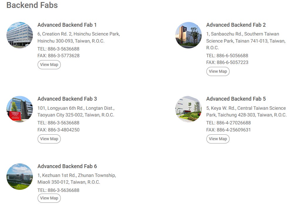
Currently, TSMC has a total of 5 advanced packaging plants located in Taiwan. AP1 in Hsinchu will become a R&D fab. AP2 in Tainan is for micro bumps and small amount of CoWoS capacity. AP3 in Longtan is mostly catered to InFO (Integrated Fan-Out), which Apple is still the main user today. AP5 in Taichung and AP6 in Zhunan are the main plants for CoWoS.
Source: TSMC
TSMC's plans to ramp up the AP7 facility in Chiayi have faced delays due to archaeological findings at the original site. As a result, the ramp-up will now take place at a 2nd site in Chiayi Science Park. Looking ahead, TSMC has ambitious plans to establish multiple advanced packaging plants in the Chiayi area.
As TSMC’s CEO C.C. Wei guided in the latest earnings call, “Talking about CAGR of those kind of increase of the CoWoS capacity, now, it's out of my mind. We continue to increase whatever, wherever, whenever I can, okay. The supply continues to be very tight, all the way to probably 2025, and I hope it can be eased in 2026”.
TSMC’s CoWoS capacity will grow from 13k wpm at the end of 2023 to 30-35k at the end of 2024 and 70-80k at the end of 2025. CoWoS capacity in 2025 is now significantly higher than the street’s estimate just a few months ago. TSMC continues to acquire more lands in Taiwan, so it is still too early to judge the final CoWoS capacity at the end of 2026. It will at least be 100k wpm by the end of 2026.
Why is so much capacity needed?
The rapid expansion of CoWoS capacity indicates that AI chipsets demand forecast of Nvidia, AMD and the system companies (Google, Amazon, Meta and Microsoft) remain very postive. CoWoS is mostly used for HPC and AI applications where HBM is integrated with the logic chip in a package. TSMC has managed to capture almost 100% market share of the AI chip market, and this has become a significant bottleneck.
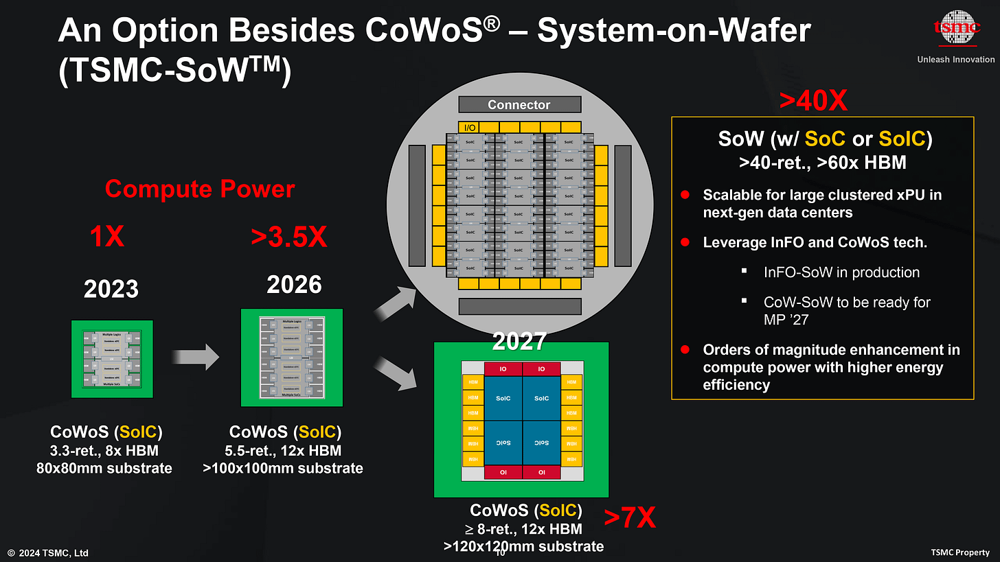
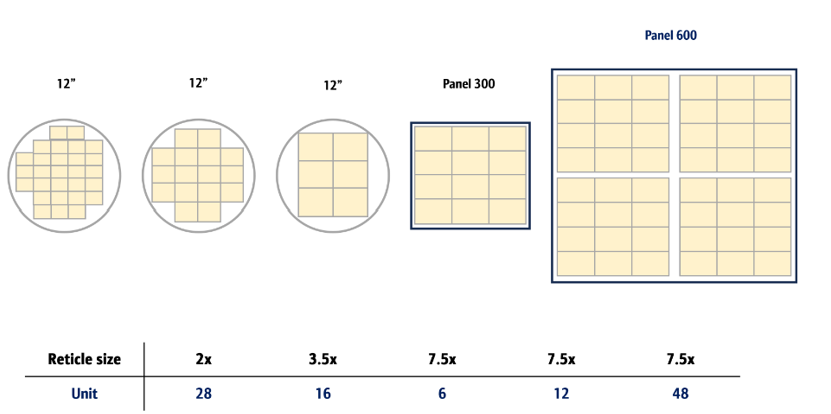
Bigger package size is an ongoing trend and TSMC is making the preparation for the bigger package. Reticle size is the biggest possible die size at 858mm2 (26 x 33mm) based on the field size and photomask. Given that many chips are at close to reticle size, making bigger package through advanced packaging is the way to go to drive higher compute performance. Blackwell at 3.3x reticle size is significantly bigger than Hopper and the next-generation Rubin will come in at 4.0x reticle size to fit 12 stacks of HBMs. The larger package size consumes more CoWoS capacity especially as you are fitting rectangles in a circle.
Source: TSMC
Source: ASE, BofA
One solution is panel level package (PLP) which will lead to smaller area loss. However, PLP is unlikely to become a mainstream solution until at least 2027 as the equipment ecosystem is not ready. Warpage and breakage are key problems that TSMC must resolve in addition to qualifying backend equipment for the bigger panel size. Equipment must be ready to handle much bigger panel of up to 60x60cm. TSMC is expected to settle on the size of the panel soon, so that the ecosystem can start preparation for it.
Equipment suppliers are obvious beneficiaries while it lasts
Given the aggressive capacity expansion, equipment vendors will do very well in 2025 with the ramp of AP7 and AP8. Key suppliers of advanced packaging equipment are ASMPT, BESI, Camtek, Onto Innovation and SUSS MicroTec. ASMPT is the market leader for TCB (Thermo Compression Bonder) tool and is awaiting final qualification for TSMC’s Chip to Wafer application. BESI is the market leader for hybrid bonder, but we are unlikely to see a big ramp in TSMC’s SoIC capacity (4k wpm in 2024 to 8k wpm in 2025) next year. Onto has a much higher share of TSMC’s advanced packaging capacity than Camtek. SUSS MicroTec is a provider of temporary bonder debonder tool and UV scanner.
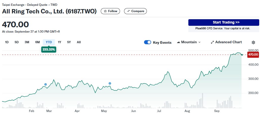
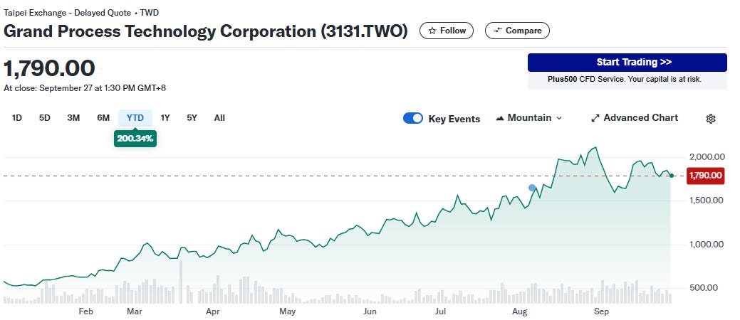
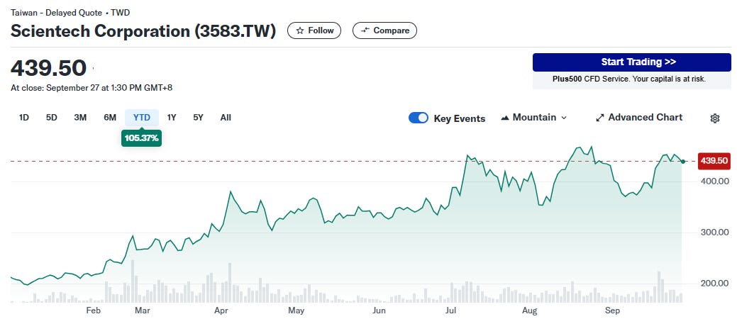
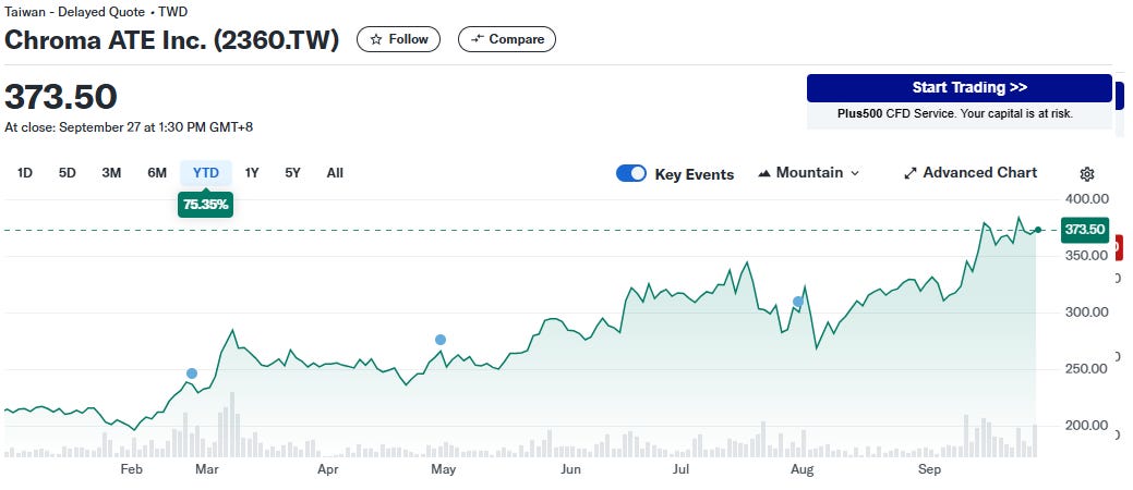
In recent months, local Taiwanese supply chain companies like All Ring Tech, Grand Process Technology Corp, Scientech, and Chroma ATE have emerged as standout performers in share price. They have achieved significant market share gains due to strong collaboration with TSMC, allowing them to align their offerings with the needs of the semiconductor giant. All Ring Tech provides underfill dispenser, AOI and heat sink machines. Both Grand Process Technology and Scientech are providers of cleaning equipment for the CoWoS process. Chroma ATE has been qualified by TSMC to be the main equipment vendor for the metrology tool for CoWoS’s redistribution layer measurement. Some of these are customised tools for TSMC, which is another barrier of entry for other foundries or OSATs.
Source: Yahoo Finance
Expectations are high and share price of related companies has gone through the roof. How long the party lasts hinge on whether TSMC will continue to expand CoWoS’s capacity aggressively in 2026 and 2027. Given that backend capex is only 10% of TSMC’s total capex, the financial risk is low for TSMC even if forecasts from customers turn out to be over optimistic. This will certainly be an important area to follow as major innovations such as hybrid bonding, co-packaged optics and panel level package are set to take off in the medium term.


Need more for AI
Need more CoWoS