TSMC A16, Hynix results (new fab, custom HBM, hybrid bonding)
A16 is SUPERior to 18A, WFE is getting better visibility
TSMC A16 - Super Power Rail is better than Intel’s Backside PowerVia
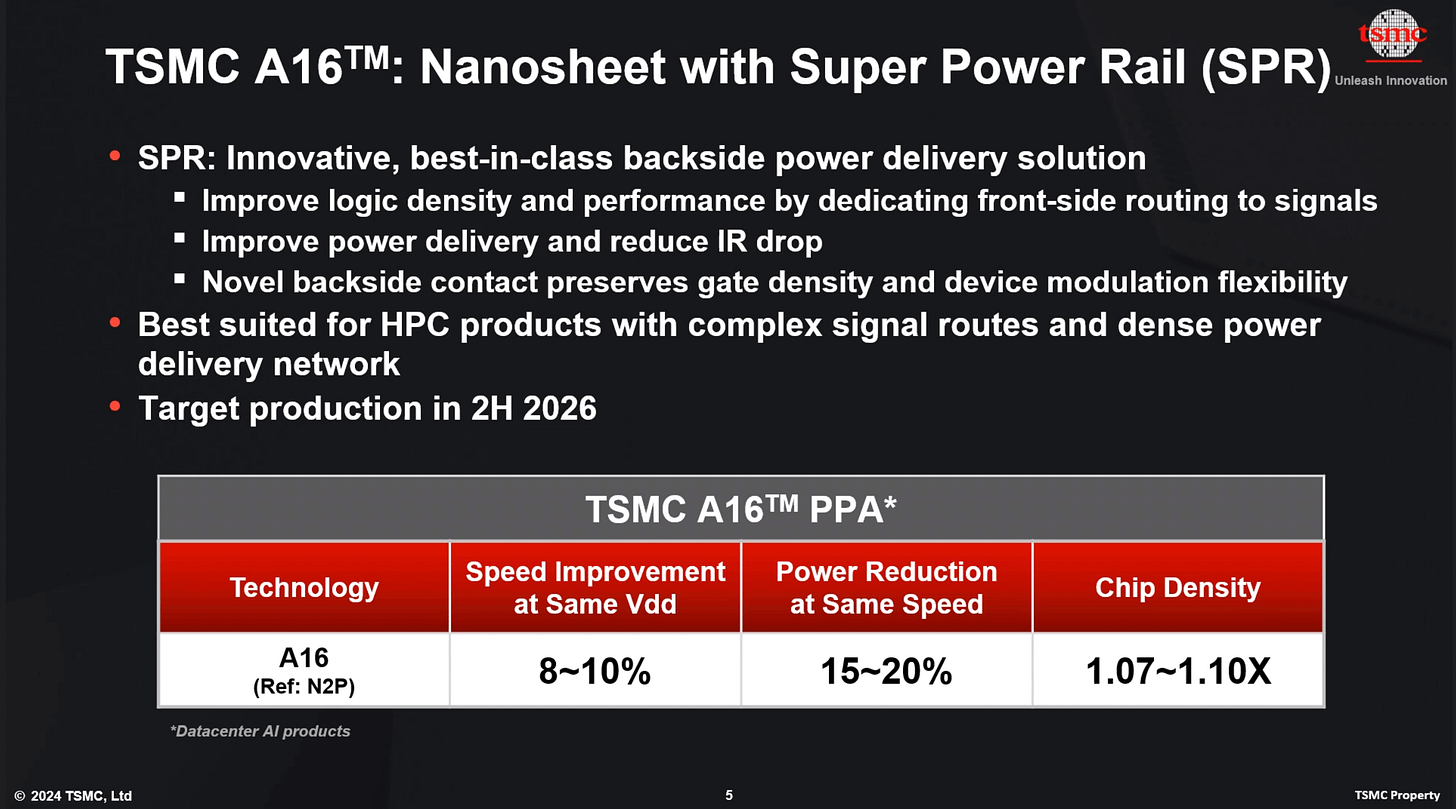
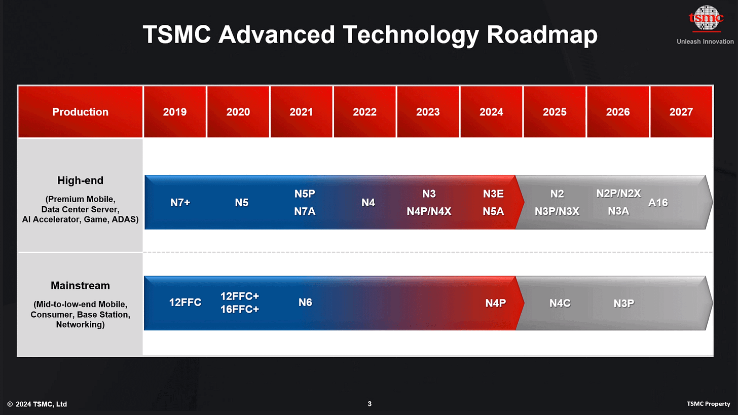
AT TSMC’s annual symposium, A16 was revealed as the next node after N2. Backside Power Rail has now been removed from N2P. A16 will be TSMC’s 1st node to combine gate-all-around (GAA) nanosheet FET with a better version of BPR called Super Power Rail (SPR). A16 will start production in 2H 2026, half a year after N2P.
This is not simply renaming N2P as A16. A16 will see high single digit density gain, 8 to 10% speed improvement at same voltage and 15-20% power reduction at the same speed vs N2P.
Intel’s PowerVia vs TSMC’s Super Power Rail
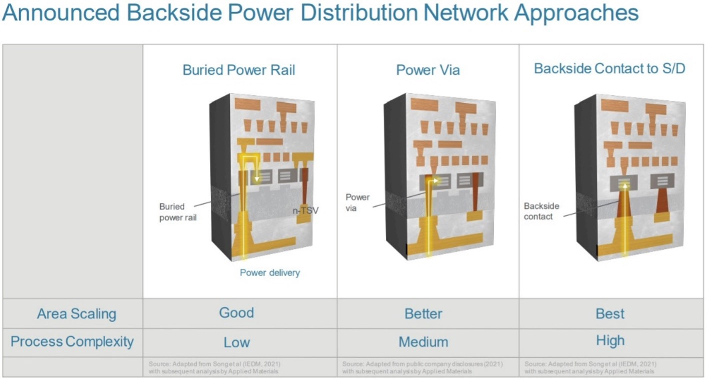
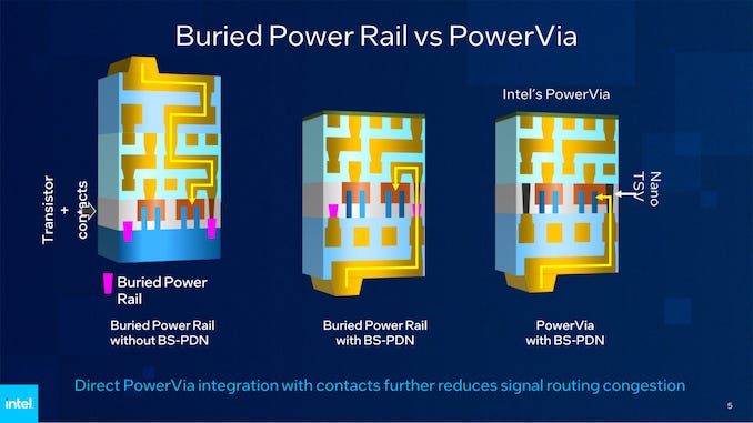
Back at AMAT’s investor day in 2022, they highlighted the differences between the different approaches to Backside Power Distribution. Intel has chosen Power Via as the technology roadmap for 20A and 18A. TSMC has decided to choose Backside Contact to S/D (Source and Drain) for its Super Power Rail. Super Power Rail has the best scaling at the cost of much higher complexity than the Power Via adopted by Intel. AMAT had talked about the differences in its masterclass in 2022.
AMAT Masterclass 2022: “The third approach is significantly more complex. We are developing integrated material solutions as well as co-optimized solutions to enable this third approach. The approach increases logic density by around 30%, which is equivalent to two nodes of EUV scaling”
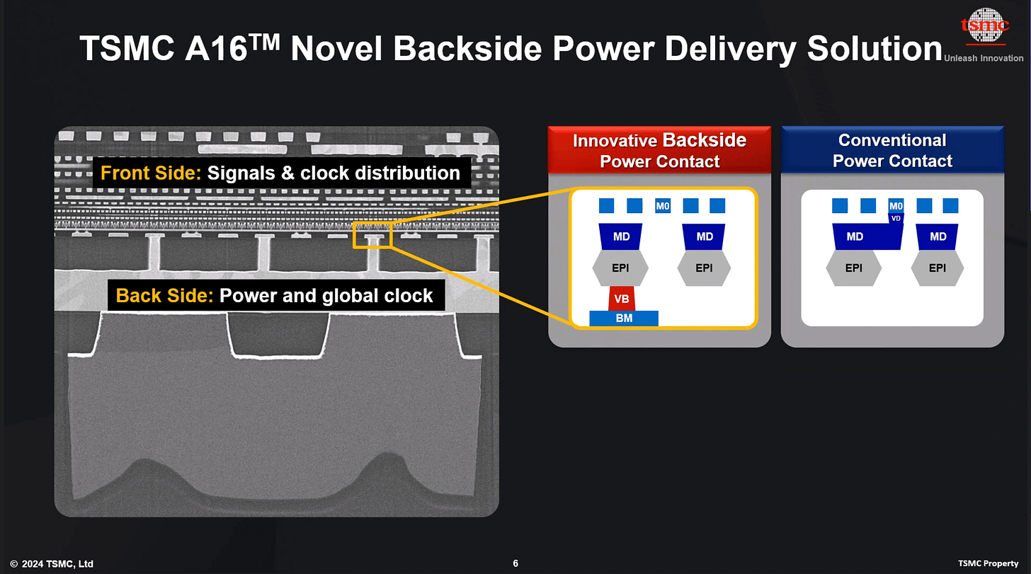
Intel uses Nano TSVs to connect the backside power network to the transistor, while TSMC’s approach is to do a direct contact of the backside power network to the source and drain of the transistors.
TSMC’s process leadership position is widening over Intel
At Intel’s Foundry Day, it was revealed that 18A will ramp in 2026 with big volume ramp in 2027. This was a slight delay from what Intel stated in 2022 Q4 earnings that 18A will achieve manufacturing readiness in 2H 2024.
TSMC 2022 Q2 earnings
“N2 deliver full node performance and power benefits to address the increasing need for energy-efficient computing, with 10 to 15% speed improvement at the same power or 20% to 30% power improvement at the same speed and logic density of more than 20% increase as compared with N3E.”
TSMC 2023 Q2 earnings
“Backside power rail will provide 10% to 12% additional speed gain and 10% to 15% logic density boost on top of the baseline technology. We are targeting backside power rail to be available in the second half of 2025 to customers with production in 2026”
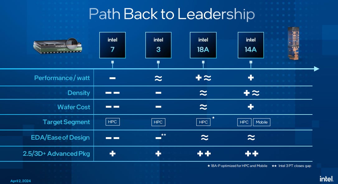
TSMC CEO has previously stated that Intel’s 18A is similar to TSMC’s N3P in PPA. N3P is TSMC’s iteration of its N3E and will ramp in very high volume in 2H 2024. Given the double-digit improvement of N2 over N3E and single digit improvement of A16 over N2, TSMC is only widening its process leadership over Intel. With only half a year of gap between 18A and A16, Intel will at most be able to secure small clients for its foundry business.
A16 could even be better than Intel’s 14A in 2028 despite Intel’s use of High-NA EUV. Pat Gelsinger: “Generally, when we say a node, it's at least double-digit power-performance improvements per node. You know, I think our cut off is 14% or 15%"
AMAT and ASMI are beneficiary of A16 with the adoption of Super Power Rail and potentially higher layer count of ALD.
SK Hynix Q1 2024 results
SK Hynix reported a gross margin of 39% which was 19% higher than previous quarter (includes 7% reveral of inventory valuation loss). DRAM ASP grew by more than 20%, while NAND ASP grew by more than 30%.
While this was a strong beat, HBM3e has yet to meaningfully contribute to its revenue yet. 8-Hi HBM3e will ramp from Q2 for H200, while 12-Hi HBM3E will be ready in Q3 2024 for GB200. With each generation of HBM having higher ASP than the previous, we are definitely far from peak earnings for Hynix.
Hynix has also confirmed that hybrid bonding has been pushed back after the height relaxation by JEDEC. Productivity and quality issues are the main concerns in the early day of adoption, while more metrology and inspection will be needed. The likely timeline for HB adoption by Hynix will be in 2H 2028 when $3.8bn Indiana plant for advanced packaging is ready.
Hynix also announced a new fab M15X in Cheongju for DRAM to be opened at the end of 2025. This was not entirely a surprise as I have written in earlier article about how Hynix is constrained by Wuxi fab. HBM3E requires the use of 1b nm, while Wuxi Fab is stuck at 1a nm due to the restriction of EUV in China. M15X has the advantage of being adjacent to the current M15, which has TSV capacity for HBM.
Is the DRAM cycle over because Hynix announced a new fab? The fab will only be ready for production in 2026. Given Micron is also opening a new fab in 2026, this does add to the risk of a reversal in DRAM pricing in 2026. We are still more than 1.5 years away, while demand for AI is looking stronger. We will likely be looking at shortage in supply before we see any oversupply.
Total investment for M15X is KRW 20 trillion (USD 14.5bn), of which KRW 5.3 trillion will be for infrastructure. M15X equipment spending will be USD 10.7 billion, which is a meaningful addition to WFE in 2026 and 2027. Since M15X is for 1b nm and beyond, ASML’s EUV will be a part of this USD 10.7 billion spend. Yong-in cluster is still ready for mass production in 2H 2027, so this is an additional investment from SK Hynix.


