
TSMC 2025 Technology Symposium
A look at semiconductor long-term demand and TSMC's technology roadmap

Each year, TSMC Technology Symposium offers important insight into semiconductor innovation. Against the backdrop of strong global AI semiconductor demand, TSMC laid out a roadmap that underscores its central role in the future of computing. Personally, I have always enjoyed the presentation made by Dr Kevin Zhang, the Deputy Co-COO and VP of Business Development at TSMC.
All slides below are from TSMC Technology Symposium. Here are the key takeaways that matter for both investors and industry watchers.
Semiconductor Market Outlook
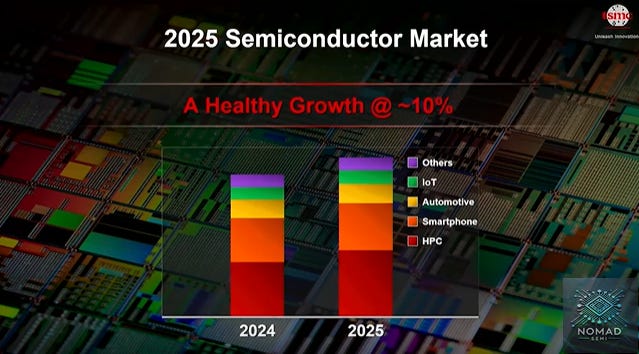
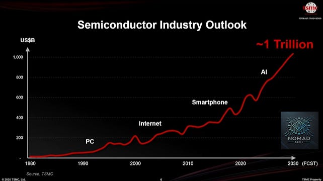
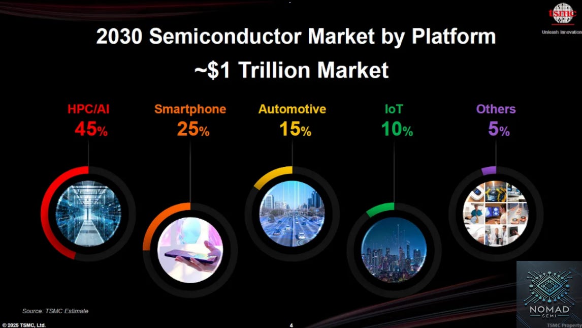
According to TSMC, they continue to expect the global semiconductor market to grow by 10% in 2025. Similar to last year, Dr Kevin Zhang affirmed that the global semiconductor market will grow to $1 trillion by 2030. HPC/AI will account for 45%, followed by 25% for smartphone, 15% for automotive, 5% for IoT and 5% for others. Based on 2024 global semiconductor sales of $621 billion, this implies an 8.1% CAGR in the global semiconductor market from 2024 to 2030. 8.1% CAGR is the fastest the semiconductor market has grown since 2000.
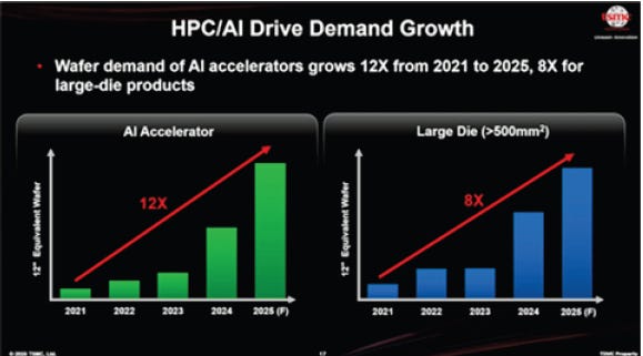
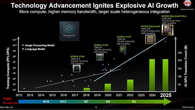
The key driver behind the strong growth outlook is driven primarily by HPC/AI application. TSMC expects HPC/AI to be a $450 billion market by 2030. In the FY 2024 results call, CEO C.C. Wei believed that their revenue growth from AI accelerators will approach mid-40% CAGR from 2024 to 2029. This is after a 12x increase in wafer demand for AI accelerators from 2021 to 2025.
Currently, all AI customers (other than the Chinese) are working with TSMC on GPU and ASICs. Majority of AI accelerators demand is on 3nm and 5nm, using TSMC’s advanced packaging technology such as CoWoS and SoIC. In the chart below, we can see the scaling of training compute achieved by NVIDIA through leveraging the latest semiconductor technology.
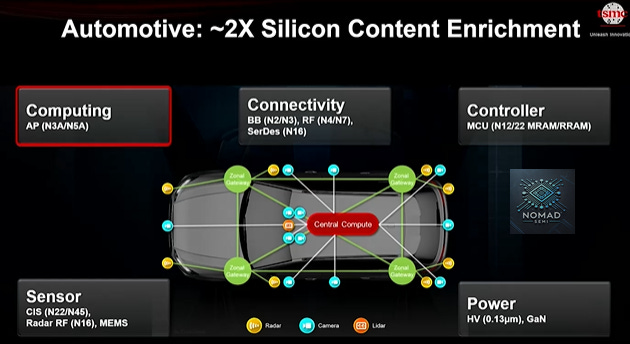
The other major growth driver identified by TSMC is the automotive application which will become a $150 billion market by 2030. While the automotive market remains soft, silicon content is growing rapidly. Rising intelligence in automotive application and higher EV penetration is a boon for the automotive semiconductor market. A lot more sensors and computing power will be needed as cars are moving towards L3 to L5. Compute is also being centralized compared to the MCU dominant setup in traditional cars. Software defined vehicle is enabled by silicon defined vehicle. Use of 3nm for automotive computing and 12nm for MCU is quite a surprising development given the current process technology node used by automotive application.
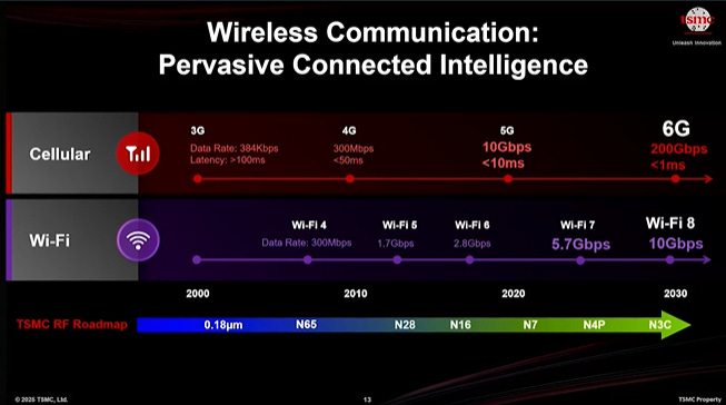
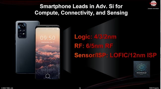
Smartphone is a stable market given unit shipment has peaked in 2016. Content growth will be the key driver as Apple, Qualcomm and MediaTek continue to migrate to the next leading-edge node. AI smartphone could drive semiconductor content in the near-term, but we will have to wait for 6G in 2030 for a big jump in smartphone semiconductor content. For Wi-Fi, 6/7nm is required to achieve the latest technology of Wi-Fi 7. Image sensor is migrating from 28nm to 12nm, while RF is also migrating to 5/6nm
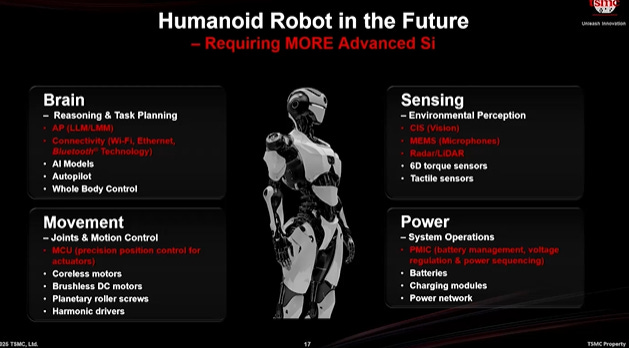
Both VR and Humanoid robot are new growth driver for global semiconductor market in the future. Many different type of semiconductors are needed to enable Humanoid such as sensor, PMIC, MCU, AP and connectivity. For VR to take off, semiconductor is required to drive 10x improvement in power, cost and form factor.

TSMC Technology Roadmap
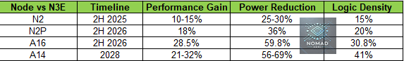
Nothing surprising on TSMC’s roadmap with their dedication to small improvement in process technology on an annual cadence. N2 will start to ramp in 2025, followed by N2P and A16 in 2026. A16 is a version of N2 that will be equipped with Super Power Rail.
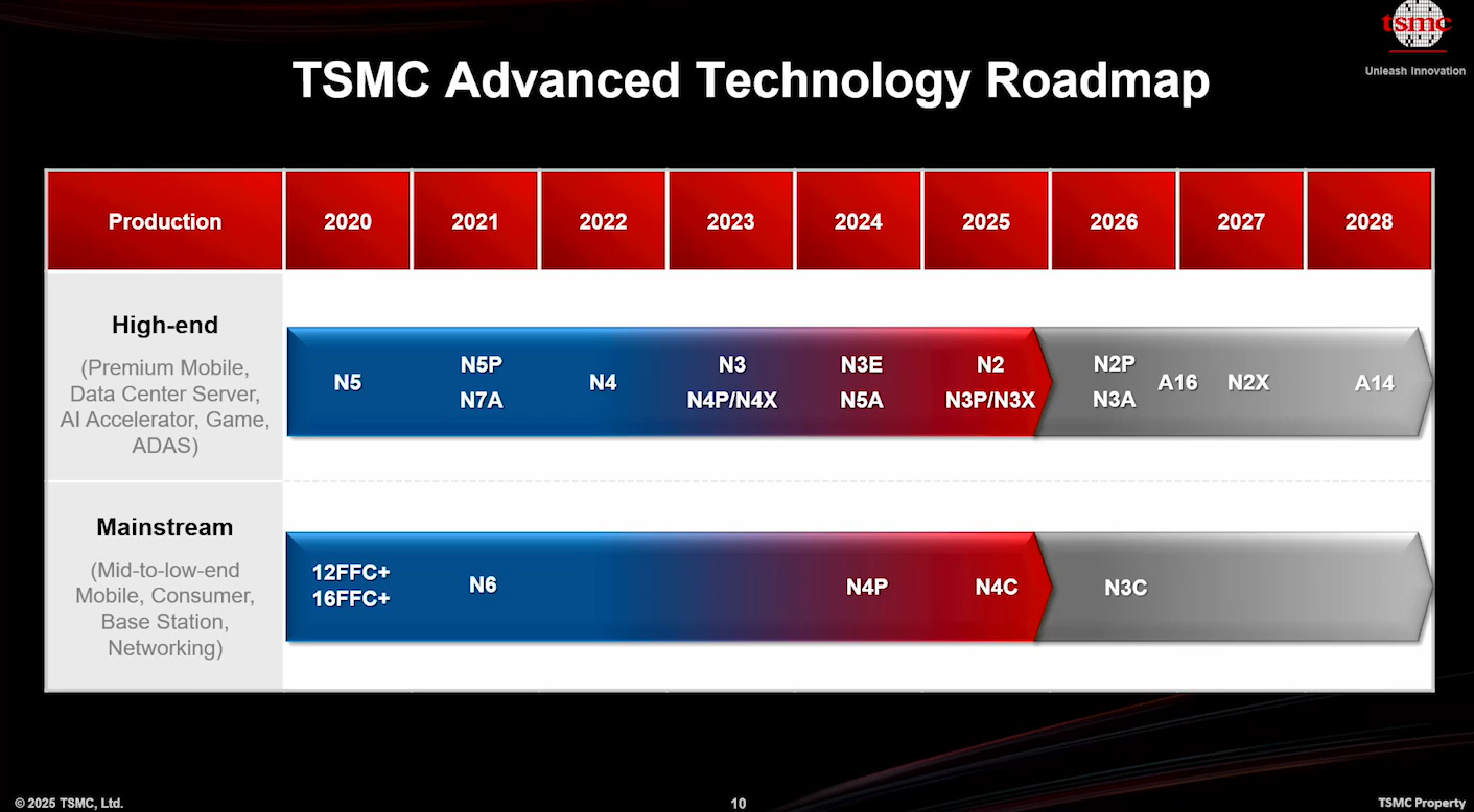
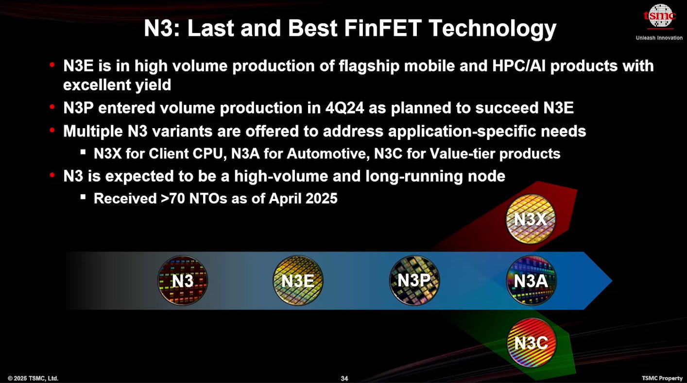
Similar to what TSMC has always done, they continue to improve on existing nodes and offer derivatives node that is more suitable for clients. TSMC has come up with N3X for client CPU, N3A for automotive and N3C for value product. Apple could be using N3C for its cheaper iPhone in the future. N3 has done really well for TSMC with revenue growth of more than 300% in 2024.
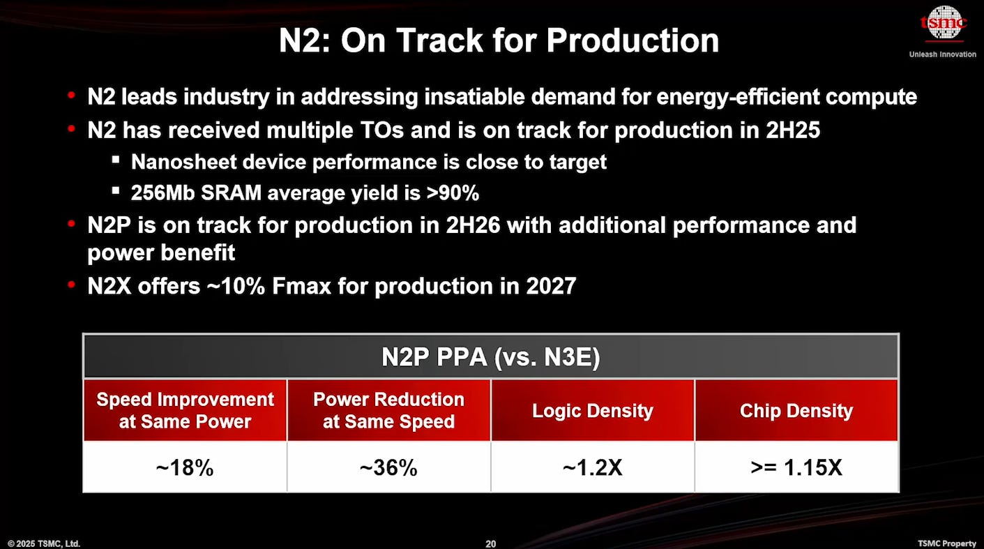
N2, which will adopt the new Gate-All-Around FET architecture, is set to ramp in 2H 2025. N2 will remain the industry leading process node, ahead of Intel’s 18A.
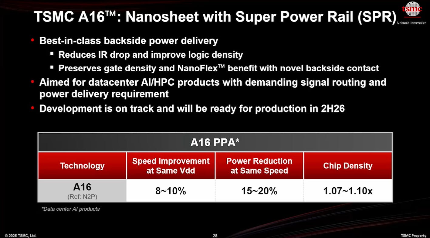
A16, which was introduced last year, will feature Super Power Rail. Super Power Rail is TSMC’s version of Backside Power Delivery (BPD) and is the hardest version of BPD. SPR is most suitable for AI/HPC product with high power requirement. OpenAI is rumored to be one of the early customers of A16 when it ramps in 2H 2026.
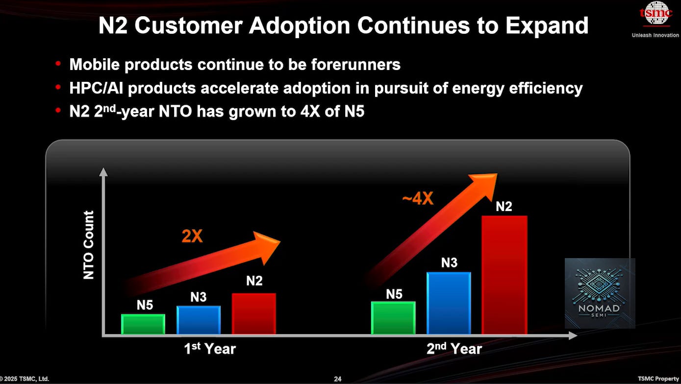
The number of new tape-out for N2 will grow a shocking 4x compared to N5 in the 2nd year. In addition to TSMC’s process leadership in N2, AI demand is likely the reason for the high number of tape-out. Google, Amazon, OpenAI, Meta and Microsoft should be looking at N2 node in 2027/28 to get a leg-up over NVIDIA. N2 is a very successful process node as TSMC has been in N3.
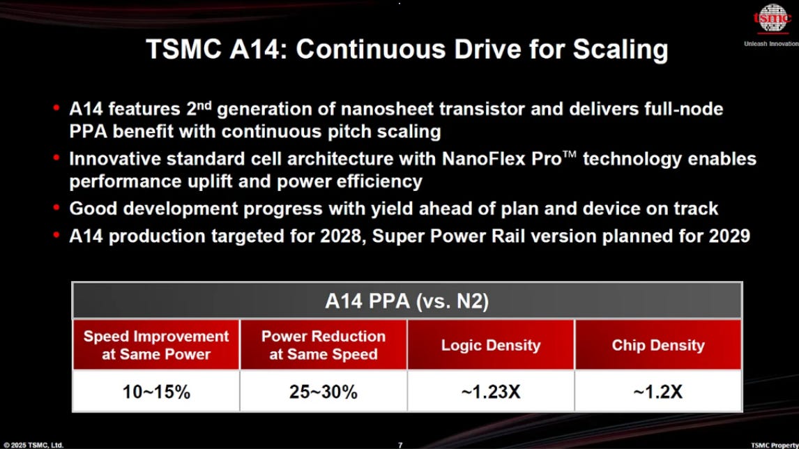
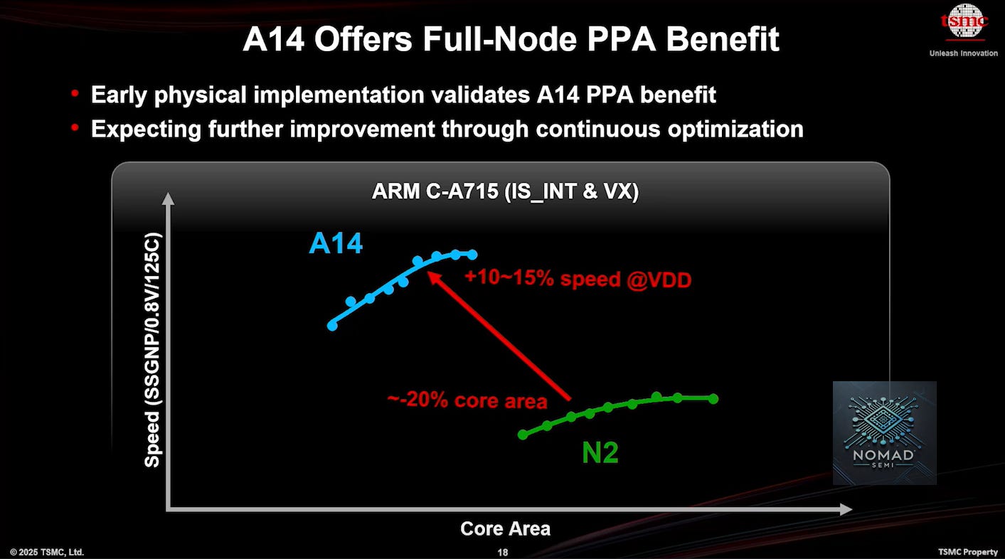
At the symposium, TSMC also introduced A14 as the next node that will enter mass production in 2028. This process builds on its nanosheet foundation and promises 10–15% performance gains and 25–30% power savings over N2. The logic density gain, speed improvement and power reduction of 14A are impressive although this is 3 years after the ramp of N2. However, the company will not include backside power delivery at A14. Instead, SPR will be offered as an option in 2029, a decision that diverges from Intel’s more aggressive adoption.
On High-NA EUV, it is unlikely that TSMC will adopt it for A14 due to cost and technology maturity issue. The likely timeline for TSMC to introduce High-NA EUV will be A10 node in 2030/31. However, A14 will see logic pitch shrink, so we are likely to see higher usage of multi-patterning with Low-NA EUV.
Comparing against N3E which was launched in 2H 2023, we can see that Super Power Rail is a great boost for TSMC’s A16 despite its higher cost.
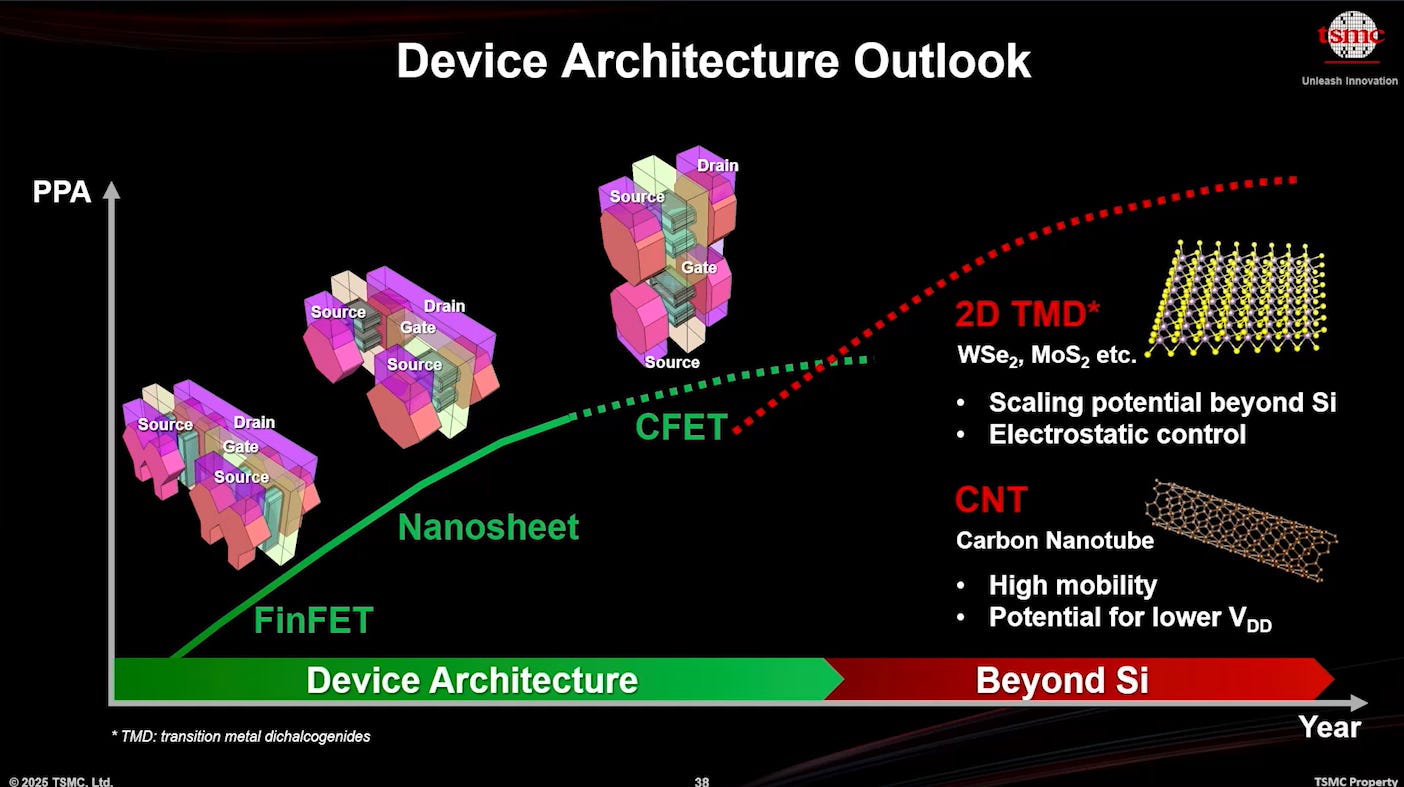
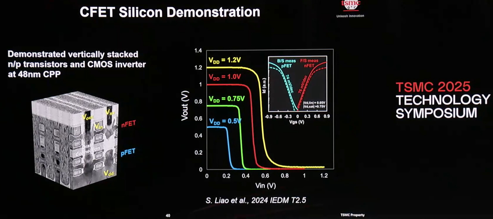
Looking beyond A14, TSMC is already doing their research on future transistors innovation. While Moore’s Law has slowed, it is by no means dead. After GAA, we still have complementary FET (CFET) and High-NA to push the PPA further. The CFET architecture will stack both the n-type and p-type transistors on top of each other. ALD and etching providers will benefit in the transition to CFET architecture. Beyond CFET, TSMC is researching into future materials such as 2D transition metal dichalcogenides (TMD) and carbon nanotube (CNT).
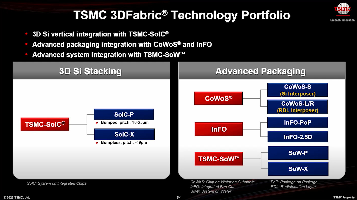
Advanced Packaging Roadmap
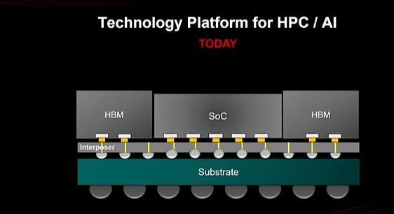
Given a slowing Moore’s Law, advanced packaging is increasingly important to achieve further scaling. CoWoS (Chip on Wafer on Substrate) has become such an important term for investors looking at NVIDIA and AI demand in 2024. InFO is one of the key reasons why Apple has sole-sourced at TSMC in the last 10 years. TSMC’s head start in advanced packaging is becoming a barrier of entry for any competitors in addition to its front-end process leadership.
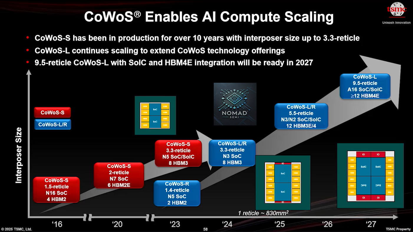
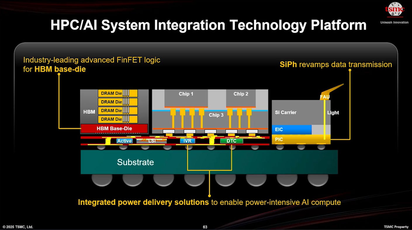
The company’s CoWoS platform continues to scale and TSMC expects to produce interposers up to 5.5x reticle size in 2026 and 9.5x reticle size in 2027. This will be able to integrate 12 HBM stacks alongside 4 AI accelerators. Rubin Ultra in 2027 is likely the 1st customer for this large package. Given that the package is now 9.5x reticle size, TSMC has also started to explore panel-level packaging solution to improve the yield rate.

Source: Data Center Dynamics
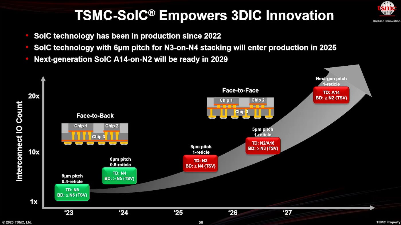
TSMC’s SoIC (System on Integrated Chips) platform will support 6um face-to-face hybrid bonding in 2025 and aims to enable A14-on-N2 chip stacking by 2029. The trajectory implies a 20x increase in I/O density in 2029 compared to the first SoIC generation. The growth of SoIC is important for BE Semiconductor investors as it will drive the adoption of hybrid bonder. AMD and Apple will use SoIC at N2 for their HPC application.
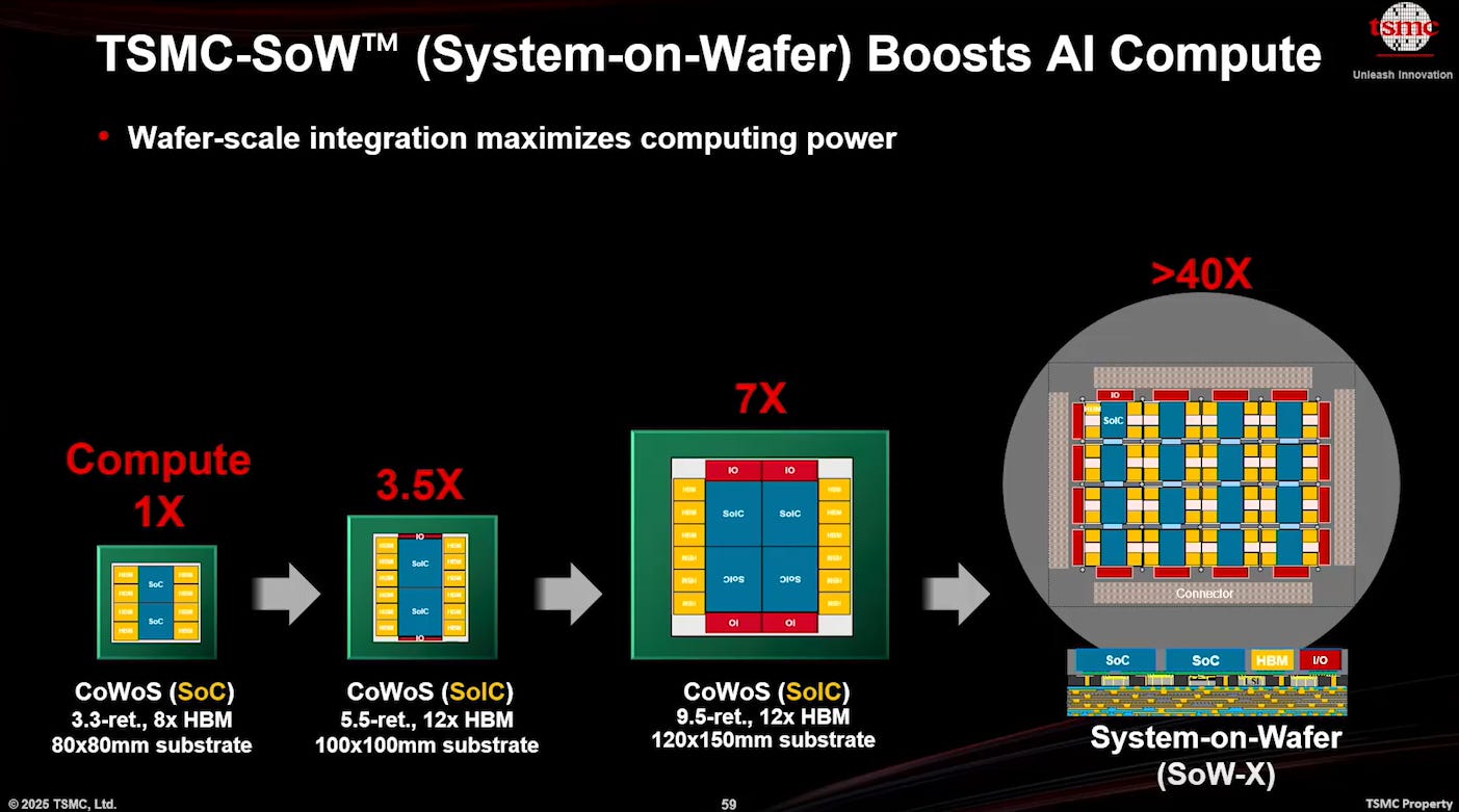
TSMC also introduces the SoW-X (System on Wafer) architecture, where wafer scale integration is achieved with CoWoS. The SoW-X platform promises over 40x the computing power of the current CoWoS package used by Blackwell and is slated for production by 2027. Unlike the current SoW-P platform which follows the chip-first approach, SoW-X will be using the chip-last approach. Companies such as Cerabras and Tesla’s Dojo have keen interests in SoW.
These architectural innovations are underpinned by a clear thesis that future performance scaling will come from advanced packaging. This is a distinct paradigm shift, and one that TSMC is leading with R&D, volume production and roadmaps. In addition, TSMC will also be introducing Co-Packaged Optics (CPO) to improve power efficiency and reduce latency of networking communication. Using photon in CPO is more energy efficient rather than electron in the current networking setup. Both Broadcom and NVIDIA are likely early adopters of CPO. TSMC is also seeking to introduce integrated power delivery in CoWoS for better power delivery density for AI application.

Source: Broadcom
Manufacturing Excellence
Dr. Cliff Hou, Deputy Co-COO and Chief Information Security Officer of TSMC, also presented on manufacturing excellence.
Defect density (D0) refers to the number of manufacturing defects found in a given area of a semiconductor wafer, typically measured in defects per centimeter square (defect / cm2). Lower defect density translates to higher yield and cost efficiency as there is higher proportion of usable chips per wafer. The trend of bigger die size also makes defect density more important as bigger die is more affected by higher defect density.
It was very impressive to hear that TSMC’s N2 defect density is better than N3 and N5 2 quarters before mass production. N2 defect density improvement is faster despite the move to the new GAA architecture.
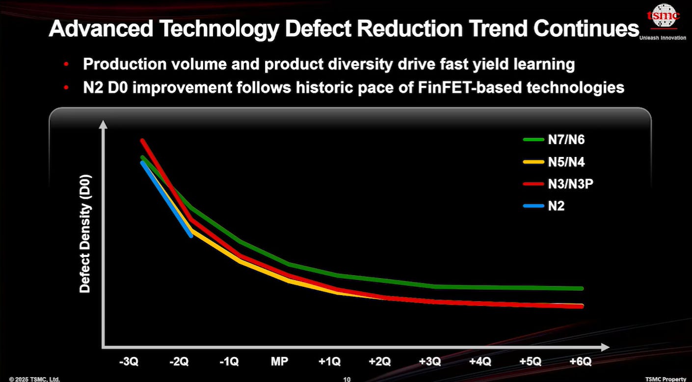
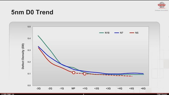
Referencing the data released at the 2020 Technology Symposium, 5nm D0 is approximately 0.2/cm2. This put N2 D0 at less than 0.2/cm2. For reference, Intel said their defect density for 18A is 0.4 back in September 2024.
Source: TSMC Technology Symposium 2020, anandtech
Conclusion
The symposium offered not just a roadmap, but a masterclass in execution. TSMC’s measured approach to node migration reflects a foundry business driven by engineering discipline over marketing hype. Customers are not after the most fancy nodes, but wants a reliable node migration that will not lead to delay in their roadmap.
The heavy emphasis on advanced packaging innovation and leadership shows how TSMC is ahead of its peers in shaping the future of semiconductor innovation.
Thank you for sharing this. Good insights!
Outstanding post filled with excellent future roadmap information. Tks!