

Memory chips sit at the heart of every digital device. They make it possible for computers, smartphones and servers to store and process information. This article will take you through two of the most important types: DRAM and NAND flash.
I will explore how they work, how they differ and why it is important for investors watching the semiconductor sector.
For the earlier deep dive on HBM, please refer to the link below
Deep Dive on HBM - by Moore Morris and Ray Wang
1. The Memory Hierarchy
Not all memory inside a device works the same way. Some types are extremely fast but can only hold a tiny amount of data. Others are much slower but offer huge capacity.
A good way to think about it, is the Memory Hierarchy. The pyramid reflects trade-offs between speed, cost, and capacity:
Fast memory is small and expensive (CPU Registers and Cache)
Slow memory is large and affordable (NAND Flash, HDD)
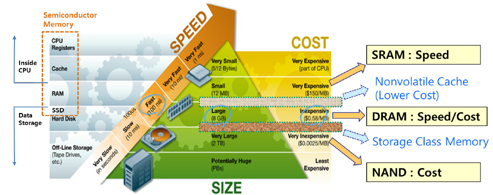
Source: Avnet
At the very top, you have CPU registers which are tiny storage inside the CPU that operate at lightning speed. Just below that are caches like L1, L2, and L3 that rely on SRAM (Static Random Access Memory). Right below is DRAM (Dynamic Random Access Memory), which serves as the computer’s main working memory. This is followed by storage such as SSD (Solid State Drive) and HDD (Hard Disk Drive) that provide massive space at much slower speeds and lower costs. At the bottom of the pyramid is magnetic tapes, which is actually still in existence today. To illustrate the difference in speed, the access time difference between each level of memory is 10x from cache to DRAM and DRAM to SSD.

Source: GeeksforGeeks
2. How DRAM and NAND Work?
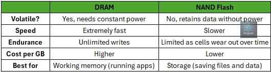
DRAM and NAND flash are both essential memory for modern electronics, but they serve very different purposes.
This is the key difference:
DRAM is volatile as it loses all data when power is turned off
NAND flash is non-volatile as it retains data even without power
Referring to the picture earlier, DRAM is Level 2 and NAND is Level 3 of the Memory Hierarchy respectively.
How DRAM Works
Every bit of information in DRAM is stored using 1 capacitor and 1 transistor. The capacitor holds an electrical charge to represent a “1” and no charge to represent a “0”. The transistor acts as a switch that connects the capacitor to the external circuit.
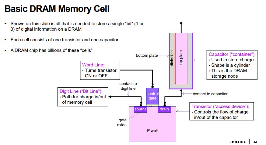
Source: Micron
However, capacitors aren’t perfect as they leak charge over time. This is why DRAM is called dynamic as they constantly need to refresh millions of times per second to maintain the data. But because it needs constant power, all data is lost instantly if the system shuts down. The benefit of DRAM is that it offers extremely fast access speeds, typically measured in nanoseconds.
How NAND Flash Works
NAND flash stores data by trapping electrons within the cell. This trapped charge changes the electrical properties of the cell, which can be detected later to read a “0” or “1.” This is known as the “NOT AND” operation.
Unlike DRAM, NAND does not need refreshing. It holds data even when power is removed, which makes it ideal for long-term storage. However, writing to NAND is slower and more complicated than writing to DRAM. You can't just flip a single bit as an entire blocks need to be erased before rewriting a new block. This means NAND is excellent for storage, but far less suitable as active working memory.
In early NAND designs, the standard structure was the floating gate. This involves the control gate that turns the cell on or off and the floating gate that stores the actual charge
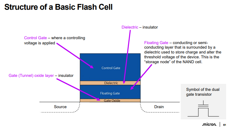
Source: Micron
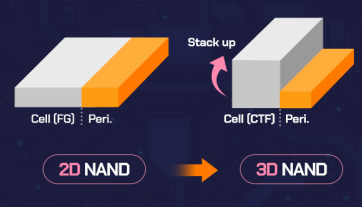
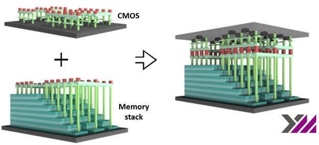
From Floating Gate to Charge Gate
Today, most of the 3D NANDs have adopted the charge gate technology. Charge trap NAND uses a silicon nitride layer to trap electrons instead of a floating gate. It’s a simpler and more scalable design, especially for 3D architectures.
The trap layer is thinner and easier to fabricate in tall vertical stacks
It reduces cell-to-cell interference which becomes a big issue in dense arrays
It’s more robust over time as chips reach 100 layers and beyond

Source: The Memory Guy Blog

Source: Stored bits
From Planar to 3D Stacking
Originally, NAND cells were laid out flat and lined up side-by-side. This is known as Planar NAND. But as we approached the limits of how small each cell could get, manufacturers started stacking them vertically. In 3D NAND, the structure looks more like a skyscraper than a city block.

Source: Enterprise Storage Forum
Source: SK Hynix
Imagine hundreds of layers of memory cells stacked vertically and all connected through vertical channels etched through the entire stack. This shift to 3D NAND allows storage capacity to increase without shrinking cell dimensions further. More bits per wafer, lower cost and continued scaling can be achieved through stacking NAND cells. Instead of using expensive lithography tools from ASML for scaling, cheaper etching tools are used.
3. A Brief History of the Memory Industry (1960s–2020s)
The story of the memory industry is full of breakthroughs, competition and shifts in leadership. As with all emerging industries, it usually takes decades before a healthy state of competition is achieved with sufficient consolidation. In the case of DRAM, it was almost 40 years!
1960s: Birth of DRAM
The 1960s laid the groundwork for DRAM. At the time, most computers used magnetic core memory that is bulky, power-hungry, and expensive. Researchers were looking for a more compact and scalable solution. In 1966, IBM’s Robert Dennard invented the modern DRAM standard with 1 transistor per capacitor.
His breakthrough was simple but elegant: use a tiny capacitor to store charge (representing a “1” or “0”) and a transistor to read or write it. This invention set the stage for DRAM to become the dominant form of main memory in the coming decades, offering far higher density and lower cost than magnetic cores.
1970s: Commercial Launch of the DRAM Industry
The modern memory industry really started in the early 1970s as Intel launched the first commercial DRAM chip, the 1103, in 1970. It replaced bulky magnetic core memory and quickly became the standard for computers.
Throughout the 1970s, U.S. companies like Intel, Texas Instruments, and Mostek dominated DRAM manufacturing. Every few years, DRAM density quadrupled following a rough early form of Moore’s Law.
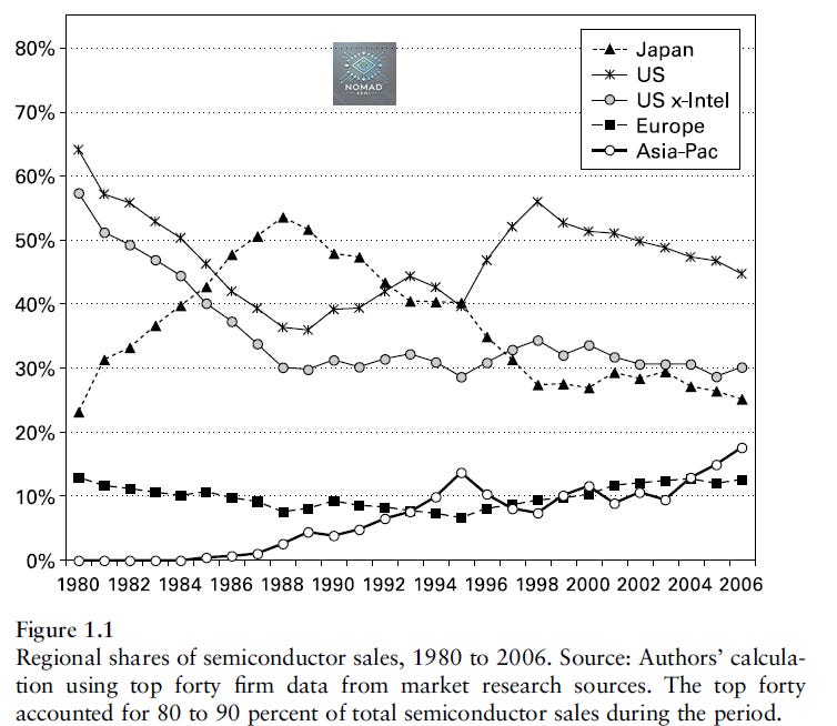
1980s: Japan Takes Over
The 1980s brought a major shift as Japanese firms such as NEC, Toshiba, Hitachi, and Fujitsu invested heavily in DRAM production. Their factories were more efficient, and their yield rates were 20-30% higher than the American rivals. This led to Japan controlling around 80% of the global DRAM market by the mid 1980s.
Source: Chips and Change
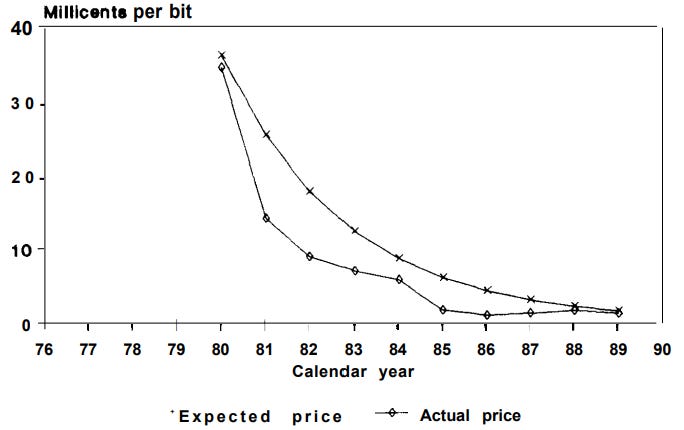
This led to intense price wars and lobbying from the U.S. memory producers. Eventually, the 1985 Plaza Accord was signed which led to a 50% appreciation of Japanese Yen over the next 2 years.
Source: Integrated Circuit Engineering Corp
Many U.S. companies simply exited the DRAM business as they were unable to compete. Then CEO of Intel Andy Grove led the company in a famous pivot away from memory and doubled down on microprocessors, changing its future forever. By the early 1990s, only a few U.S. companies are still involved in memory.
Meanwhile, a Toshiba engineer named Fujio Masuoka invented a new kind of memory called NAND flash in 1987.It wasn’t a big deal yet, but it would become the foundation for modern storage years later.

Source: Engineering and Technology History Wiki, photo of Fujio Masuoka
1990s: Korea Rises and NAND Grows
In the 1990s, another wave of competition arrived from South Korea. Samsung and Hyundai Electronics (later SK Hynix) aggressively built out memory fabs with strong government support. They focused on scaling and low costs, allowing them to start taking market share from Japan.
Meanwhile, NAND flash moved closer to reality. Samsung and Toshiba began producing early NAND chips at small density.
The seed of consolidation for the memory industry was planted near the end of the decade with the onset of Asia Financial Crisis in 1997. Under the pressure of the South Korea government, LG Semiconductor and Hyundai Electronics merged to become Hynix eventually. Elpida was formed in 1999 with the merger of the DRAM operation of NEC and Hitachi in Japan. Micron completed the acquisition of TI’s memory business in 1998.
At the end of the decade, big DRAM players remaining were Samsung, Hyundai, Micron, Elpida and Infineon.
2000s: The Flash Explosion
In the early 2000s, NAND flash demand exploded. Digital cameras, USB drives, and later smartphones needed a compact non-volatile storage solution.
Further consolidation in DRAM happened during the Great Financial Crisis. In 2008, Micron acquired 35.5% stake in Inotera, which is a JV of Qimonda (Infineon) and Nanya Tech. The next year, Qimonda filed for insolvency protection. 4 major DRAM companies remain: Samsung, Hynix, Micron and Elpida.
2010s: Start of the DRAM Oligopoly and the rise of 3D NAND
The DRAM downcycle in 2011 was the trigger of the final consolidation. In 2012, SK Telecom emerged as the sole bidder for Hynix for $3 billion and it was how Hynix became SK Hynix.
Elpida, Japan’s last hope in DRAM, eventually went bankrupt and was bought by Micron in 2013. In addition, Micron also bought out the remaining stakes in Inotera and acquired Rexchip (JV of Powerchip and Elpida).
An oligopoly emerged for the DRAM market as Samsung, SK Hynix, and Micron together controlled 90% of the market.
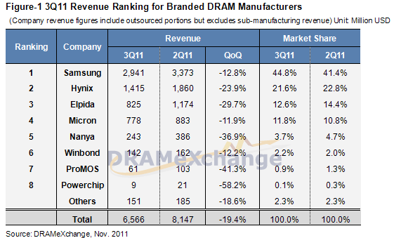
Source: DRAMeXchange
In NAND, Samsung led, but Toshiba, Western Digital, Micron, Intel, and SK Hynix kept the field highly competitive.
One huge technology shift changed everything: 3D NAND.
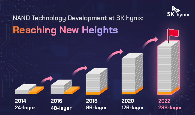
Instead of shrinking cells horizontally, manufacturers began stacking memory cells vertically. Starting with 24 layers, this became 48, 96, 200 and beyond. This solved the limits of planar scaling and dramatically increased storage capacity. By the late 2010s, 3D NAND had completely taken over the market.
2020s: HBM and China
Today, the memory landscape faces new forces as China is trying to build its own memory industry. Companies like YMTC and CXMT have started shipping competitive NAND and DRAM products respectively. They’re still behind leaders like Samsung and Micron in technology, but they’re moving fast.
At the same time, memory remains highly cyclical as always. After the memory “supercycle” in 2017-18, another bust hit in 2019. Another sharp downturn came in 2022.
The rise of AI and HPC has fueled demand for specialized memories such as HBM (High Bandwidth Memory).
4. The Current Competitive Landscape
Today, the memory business isn’t crowded as it is mostly controlled by a handful of giants. This was a huge contrast to the 1980s where almost every semiconductor companies globally produced memory chip.
DRAM
Three companies dominate the DRAM market: Samsung (South Korea), SK Hynix (South Korea) and Micron Technology (U.S.). Together, they control about 95% of the world’s DRAM revenue.

For more than 3 decades, Samsung led in market share and technology leadership. Samsung’s strong balance sheet, diversified businesses and cost leadership allow them to weather through all the previous downcycle. However, no one in the industry ever expects Samsung to lose its position as market leader in 2025.
In Q1 2025, SK Hynix is the new market leader with more than 36% revenue share of the DRAM industry. This is achieved through its dominant market share in AI-fueled HBM demand and a declining DRAM spot price. The price of an HBM chip is 5 to 10x more expensive than DDR5 on a per bit basis.
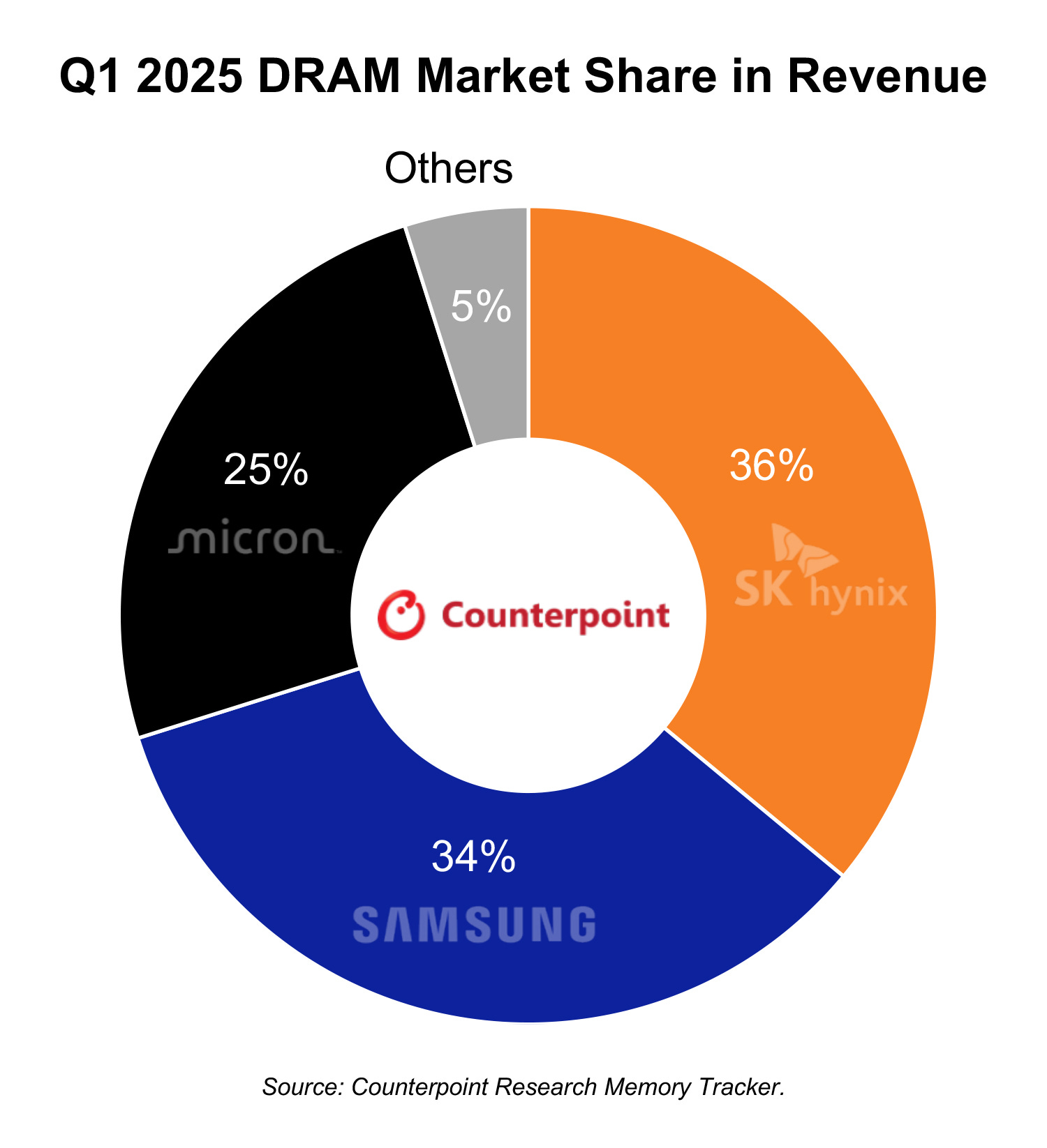
Source: Counterpoint
Micron is the up-and-coming player with a better yield rate in HBM than Samsung. Historically, the company has done best in capital allocation by acquiring capacity for cheap during the downcycle.
Ever since the acquisition of Elpida in 2013, the industry’s return on capital has improved tremendously. These days, it is common to see DRAM companies commenting on production cut or capacity upgrade during DRAM downcycle. While it remains cyclical as always, the 3 companies are now earning a through-cycle return above the cost of capital. True return for the DRAM operation is likely higher than the figures below as the 3 companies have NAND businesses. An investment in the memory companies at below book value is likely to pay off.
Source: Nomad Semi
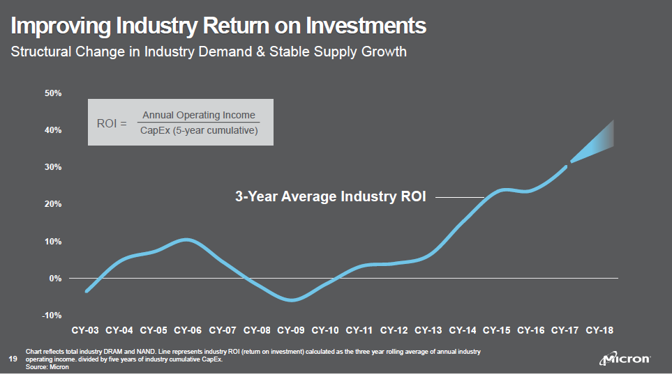
Source: Micron
NAND
Unfortunately, the NAND industry is not as profitable as DRAM although it is just 1 consolidation away.
The NAND flash is still an oligopoly, but with 5 different companies
Samsung
Kioxia (spun out of Toshiba)
Sandisk (spun out of Western Digital, partner of Kioxia)
SK Hynix
Micron

Source: Trendforce
Samsung is still the leader in NAND although the cost advantage is narrowing.
In 2021, SK Hynix acquired the Solidigm operation from Intel as then-CEO Pat Gelsinger wanted to raise money to fund the foundry business. The combined business made SK Hynix the 2nd largest company in NAND.
That merger sparked speculation on whether the Micron or Western Digital will make a move to avoid being left behind. Without further acquisition, Micron will be uncompetitive in NAND as its market share today is only 12%.
Kioxia and Sandisk enjoyed a unique partnership through their joint venture. Kioxia controls 100% of the fabs and operation of the NAND business. Through the JV, Kioxia and Sandisk split the output as well as the cost of capital expenditure & R&D. Wafer output from Kioxia operation is split 50-50 between Kioxia and Sandisk.
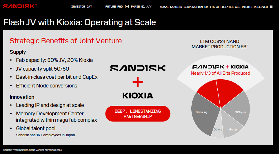
Source: Sandisk
Both Kioxia and Sandisk are the weakest player in the industry as they do not have a profitable DRAM business to fund them through the cycle. They have been losing market share to Samsung and SK Hynix over time. The first step for a merger between Kioxia and Sandisk has been taken through the IPO of Kioxia and spin-off of Sandisk.
Without a profitable business to finance them through the cycle, Kioxia is increasingly facing the stress of increasing capacity. Well-known activist investment firm Elliot was the one who pushed Western Digital to spin-off Sandisk. Meanwhile, Kioxia is controlled by Bain Capital in a consortium that includes SK Hynix. SK Hynix had previously rejected the merger deal as they claimed the deal undervalued their investment in Kioxia.
The Rise of China Memory Competition
China doesn’t want to rely on foreign memory makers and has been making efforts in domestic substitution. Two key players have emerged with CXMT (ChangXin Memory Technologies) in DRAM and YMTC (Yangtze Memory Technologies) in NAND.
Back in 2016, there were 2 main companies (Fujian Jinhua Integrated Circuit and Innotron) focusing on DRAM production in China. In 2018, Fujian Jinhua was put on the U.S. BIS Entity List, which meant it could no longer buy semiconductor equipment with U.S. technology. In a separate lawsuit, Micron sued Fujian Jinhua and UMC for stealing its memory IP.
The other company was Innotron, which was based in Hefei. Innotron was established in 2017 as a JV between Hefei government and China Integrated Circuit Industry Investment Fund. In 2019, Innotron changed its name to CXMT.
To avoid similar lawsuit as Jinhua, CXMT licensed its IP from Qimonda and Rambus. CXMT started producing DRAM around 2020 and has been growing its capacity rapidly since 2023.
There are concerns whether CXMT’s rapid capacity growth will be a threat to the oligopolistic nature of the DRAM market. By the end of 2025, it is estimated that CXMT will achieve a capacity of 300k wpm. This will be equivalent to 15% of the global DRAM capacity. Backed by Chinese government subsidies, CXMT has also started to sell DDR4 more actively to the Chinese smartphone OEMs. This was one of the concerns raised when memory prices took a turn last year.
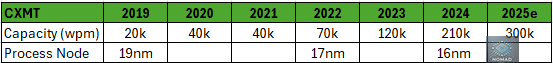
However, the good thing is CXMT is still behind the main DRAM companies in terms of technology. At 16nm, CXMT is closer to 1z nm. For reference, both Samsung and Hynix are working on mass production of 1c nm at the end of the year. By process technology, the DRAM oligopoly is still 3 generations ahead of CXMT (1z → 1a → 1b → 1c nm).
According to Techinsight, CXMT latest 16nm chip has a bit density of 0.239Gb per mm square. This is 40% lower bit density than the average of 0.4-0.45Gb per mm square achieved by the DRAM oligopoly. As a result of the 40% lower bit density, the actual bit market share of CXMT is around 5-6% despite having 15% of global capacity share. Right now, CXMT is still mostly shipping DDR4 products rather than the DDR5 products from the global companies.
Another issue that CXMT faces is its ability to continue to migrate to the next process technology. In the latest restriction, the U.S. government has further restricted equipment access for DRAM production from a threshold of bit density of > 0.288Gb / mm square to a bit density of >0.20Gb / mm square. This was a loophole that had allowed CXMT to produce at 1z nm despite the 18nm restriction for DRAM.
The other major player is China’s leading NAND producer YMTC, which has a competitive 3D NAND product. Founded in 2016 under the Tsinghua Unigroup umbrella, YMTC had received billions in funding.
Unlike many Chinese semiconductor firms, YMTC didn’t aim to merely replicate existing technologies. It created an independent path by coming out with a novel proprietary NAND flash architecture called Xtacking in 2018. Instead of fabricating the memory cell array and the peripheral logic circuitry on the same wafer, YMTC builds them separately and then bonds them together. This is achieved through a wafer-to-wafer hybrid bonder.
Source: Semiconductor Digest
As the logic and memory layers are fabricated and optimized independently, this enables a much faster read and write speeds. By offloading logic to a separate wafer, better die area efficiency is achieved as the memory array can be more densely packed. Despite the limitation of equipment access, YMTC is able to achieve a bit density nearly on par with the global giants.
Source: Techinsights
In an endorsement of Xtacking architecture, Kioxia had announced the adoption of a similar CMOS directly Bonded to Array for their 8th Gen BiCS Flash. SK Hynix is also exploring a similar technology roadmap at the moment. This is great news for wafer-to-wafer hybrid bonder providers such as EV Group and Tokyo Electron.
")
Source: Kioxia
Unlike CXMT, YMTC has more success due to its independent technology roadmap. Not only is it suppling entry level SSD products, it is also supplying enterprise grade SSD. By NAND bit share, YMTC should have a market share of 7-8% in 2024.
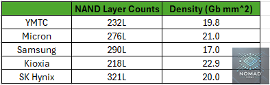
Despite the great success enjoyed by YMTC in its memory technology innovation, the firm was placed on the Entity List in December 2022. This restricts U.S. firms from supplying to YMTC without a license. Key vendors like LAM Research, Applied Materials and KLA were forced to halt shipments of essential tools. This led to a stalled 232L 3D NAND roadmap and slower capacity expansion.
However, not all is lost as China’s domestic supply chain is working hard to provide the key semiconductor equipment. In particular, AMEC plays an important role in delivering high aspect ratio etching machine as this is essential for 3D stacking in NAND. AMEC is able to achieve a 60:1 aspect ratio with their CCP etching tool and is aiming to achieve 90:1 aspect ratio next. According to Kokusai, YMTC is starting to accelerate its capacity plan again this year and is aiming for production of 200-300L 3D NAND.
Given the huge market in China, it is inevitable that both CXMT and YMTC will increase their bit share going forward. It is critical to track their progress as they could threaten the current oligopoly status of the global memory market.
5. How DRAM and NAND Are Scaling Today
For years, memory chips got better mainly by shrinking as smaller cells meant more bits per wafer, lower costs and better performance. But that simple formula started running into hard limits.
Now, both DRAM and NAND have taken on new scaling paths.
DRAM Scaling
DRAM scaling has always been tricky. Every DRAM cell needs a capacitor to store charge and that capacitor has to hold enough electrons to tell a "1" from a "0".
As cells got smaller, it became harder to build capacitors with enough storage. At the same time, wires got narrower, increasing resistance and slowing things down.
Source: Micron
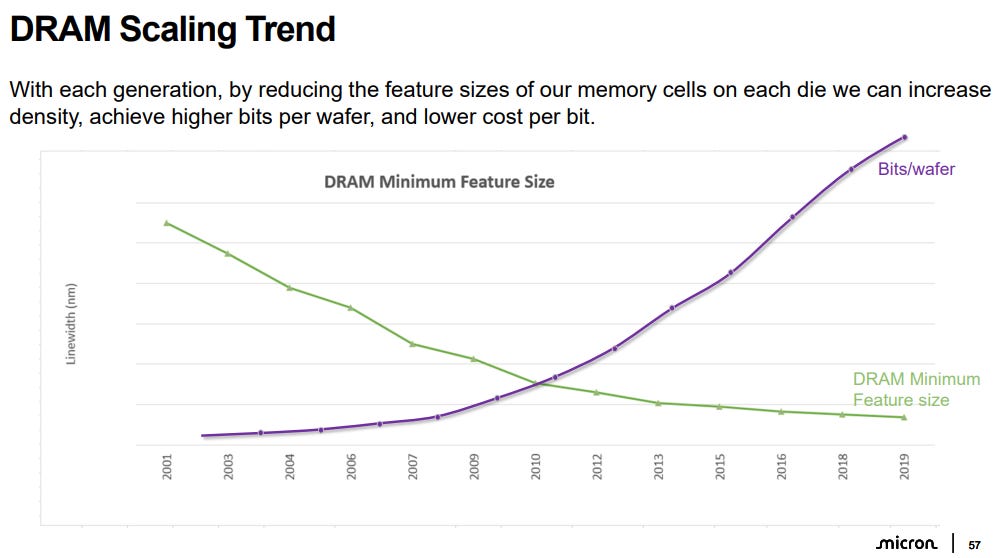
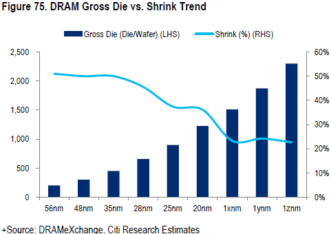
In the past, DRAM density doubled roughly every 2–3 years. From 2000 to 2010, DRAM node sizes shrank from 180nm to 40nm, which is a 4x density increase in a decade. Since 2015, node shrink has become incrementally slower from 28 nm to 1c nm today. These days, node migration only delivers 10 to 15% in density gain per generation. One benefit of the slower node shrink is that it is harder for memory companies to increase supply without incremental greenfield capex. Supply is much more predictable.
Source: Citi
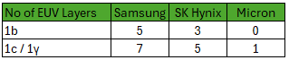
To deal with this, DRAM makers like Samsung, SK Hynix, and Micron have adopted EUV on their newest nodes. EUV helps to pattern finer features without the need for multi-patterning. Both Samsung and SK Hynix have adopted EUV at 1a nm, and are increasing EUV layers count as they progress towards 1b and 1c nm. Micron will be introducing EUV at 1-gamma at its Hiroshima plant.
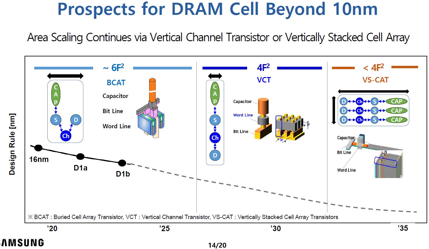
Beyond the next generation 1d nm, there is visibility to the future DRAM scaling roadmap. DRAM will transition from 6F2 to 4F2, before it migrate to 3D DRAM in 2030s.
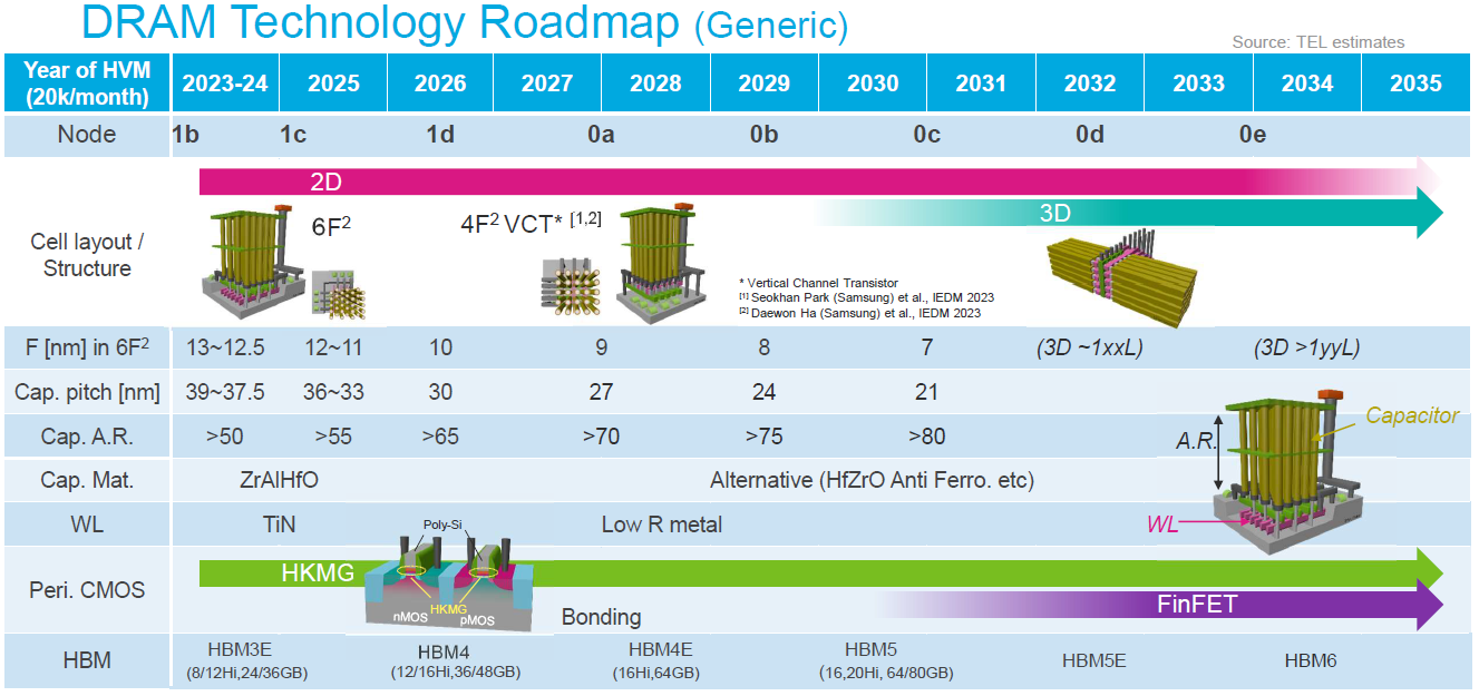
Source: Tokyo Electron
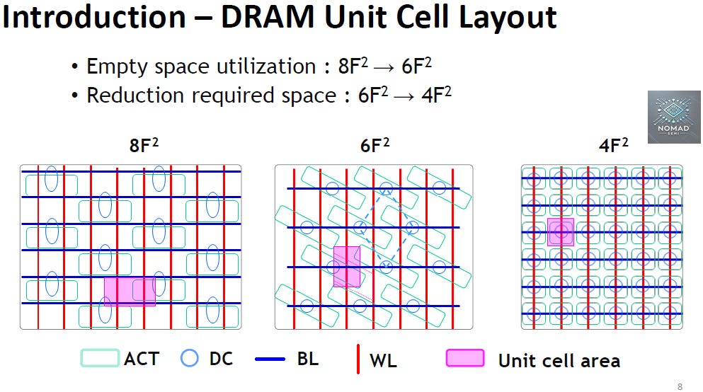
4F2 refers to the dimension of a single DRAM cell at 2F x 2F, where F is the minimum feature size of the manufacturing process. This is the smallest possible DRAM cell size. Both Samsung and SK Hynix will adopt 4F2 as they migrate into <10nm. Samsung has called it Vertical Channel Transistor (VCT), while SK Hynix has named it Vertical Gate (VG).
Source: Samsung
The new 4F2 design reduces the footprint of each memory cell by approximately 30% compared to the older 6F2 layout while maintaining the same lithography node. This is due to a more compact structure through stacking the drain, channel, source and capacitor vertically. This approach not only increases cell density, but also improves power efficiency. Cost saving is also achieved from savings in lithography cost.
Source: Samsung
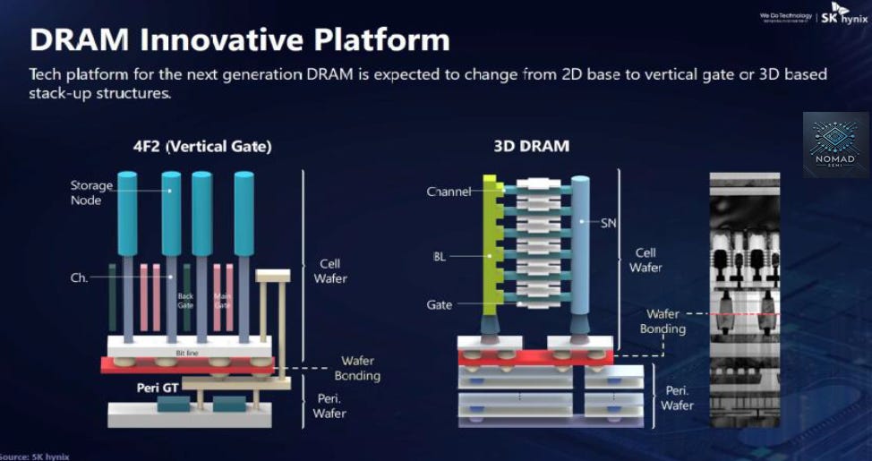
Source: SK Hynix
The next evolution will be 3D DRAM where memory cells are now stacked vertically within the chip. Samsung has called its 3D DRAM technology as Vertically Stacked Cell Array Transistors (VS-CAT) or (VS-DRAM).
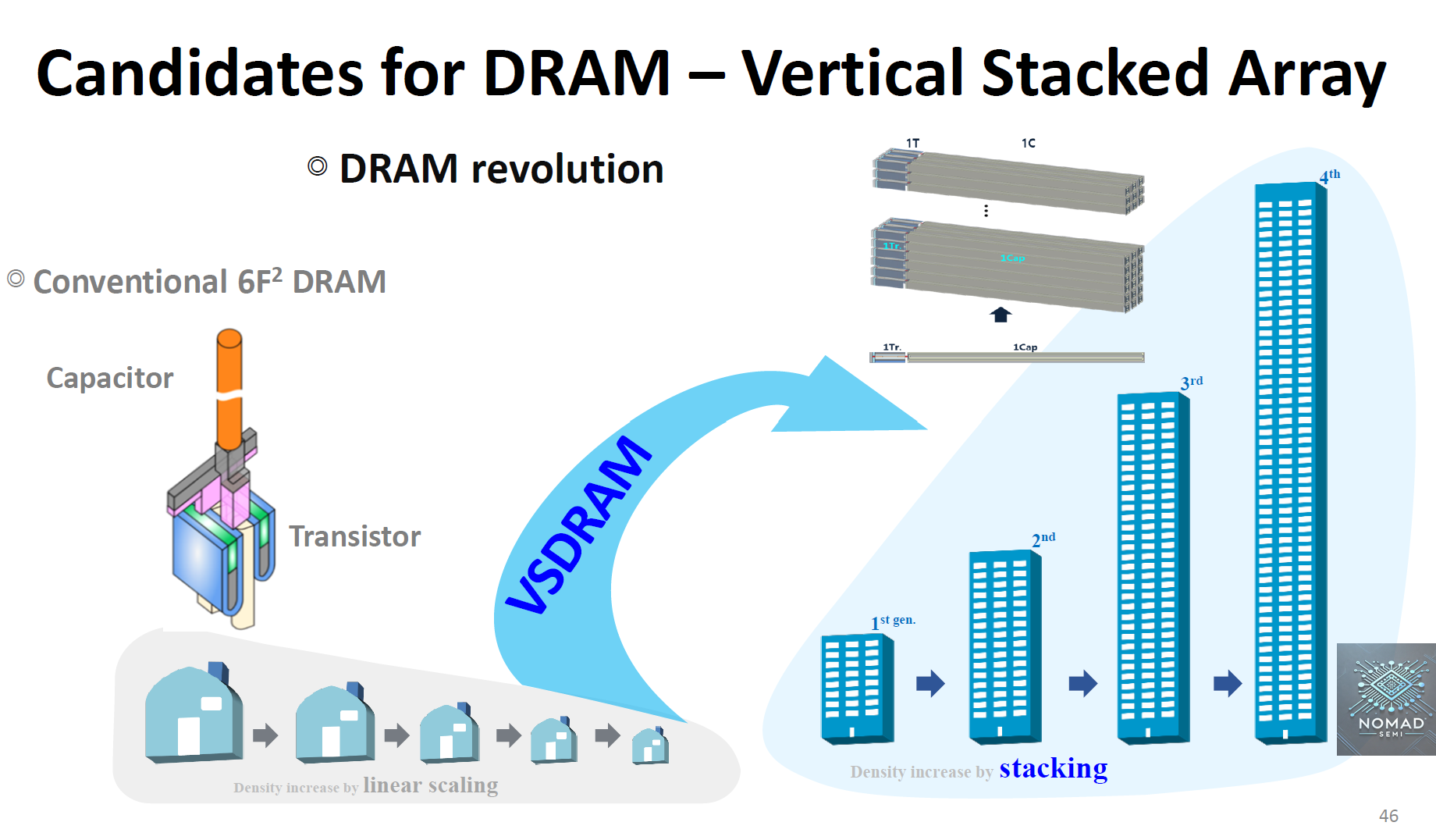
While 3D DRAM is still years away, it will reduce litho intensity significantly. On the other hand, 4F2 may maintain or reduce the litho intensity. Key beneficiaries will be current etching and deposition equipment providers such as Lam Research, Tokyo Electron and ASMI. 3D DRAM is much more complicated than 3D NAND stacking, so the exact implementation timeline remains uncertain.
NAND Scaling
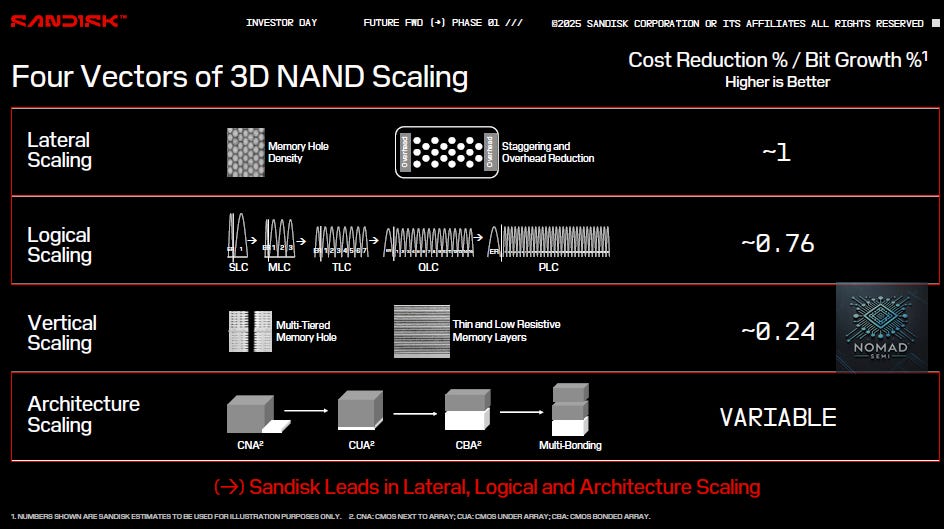
Source: Sandisk
The 1st scaling method is lateral scaling which is packing more bits per memory layer. However, this is really difficult as density increase leads to higher cost, cell to cell interference and impact data retention.
NAND flash found a better way forward through stacking layers known as 3D NAND. Instead of shrinking cells further, engineers started building memory cells on top of each other. Samsung was first to market with 24L 3D NAND back in 2013. Now, leading chipmakers have produced over 200 layers 3D NAND with 300+ layers coming soon.
Source: SK Hynix
More layers = more storage without shrinking the cells too much. Horizontal pitch shrinking has taken a pause since the advent of 3D NAND. It solves a lot of scaling headaches although building tall stacks brings its own challenges that has to be solved by better etching tools.
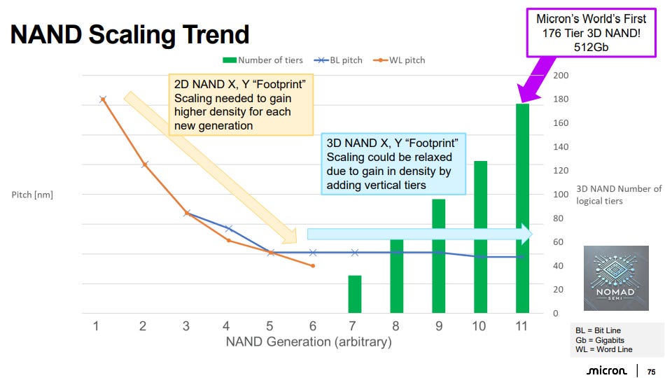
Source: Micron
For now, the roadmap is clear, which is to continue stacking up to 1000 layers by 2030. Previously, we have done a deep dive on Tokyo Electron whose cryogenic etching will be a key technology to achieve high aspect ratio etching for 1000 layers 3D NAND.

Source: Tokyo Electron
Another method is logical scaling, which involves squeezing even more bits into each cell. Originally, each cell holds a single bit, also known as SLC (Single-Level Cell). But manufacturers realized that by precisely controlling charge levels, they could store more bits per cell:
2 bits per cell → MLC (Multi-Level Cell)
3 bits per cell → TLC (Triple-Level Cell, now the mainstream)
4 bits per cell → QLC (Quad-Level Cell, growing in adoption)
5 bits per cell → PLC (Penta-Level Cell)
Bits per Cell: SLC → MLC → TLC → QLC → PLC
While more bits per cell can reduce cost, it also slows down write speeds and lower endurance since reading and writing becomes more sensitive to voltage shifts and noise. That’s why high-end SSDs still use SLC or TLC, while QLC and PLC target cold storage or low-write applications. Logical scaling gain is also getting lower as it is only 25% gain moving from QLC to PLC.
The last method is architecture scaling in a method similar to the Xtacking architecture that YMTC has adopted. SK Hynix is also considering 4D NAND, which uses hybrid bonding to stack the memory cell on top of the peripheral circuit.

6. Memory Market and Demand
Few years ago, the DRAM market is equally split between PC, mobile and data center. After Generative AI demand took off in 2023, it is now a major new driver of DRAM demand. Higher DRAM bandwidth is required to prevent bottleneck during AI training and inferencing. With the rapid growth in AI, data center will account for 2/3 of the DRAM bit demand in 2029. Assuming a single digit annual decline in DRAM ASP and high teens bit demand growth, the DRAM market is expected to grow at mid to high single digit over the next few years.
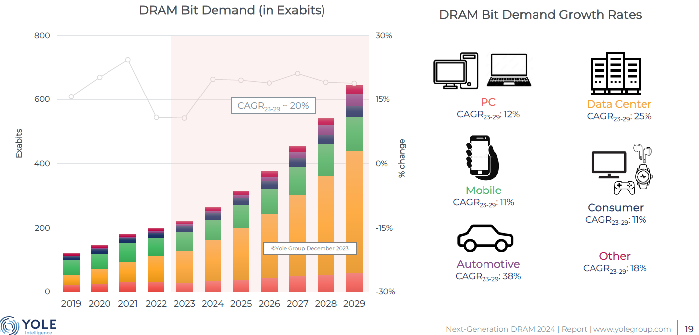
Source: Yole
NAND demand has slowed down from the high 30s during the 2010-20 decade and we are looking at high teens bit demand growth going forward.
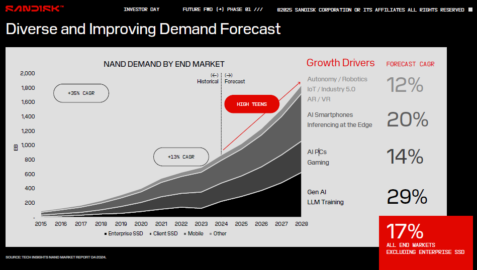
Source: Sandisk
7. Other Memory Technologies to Watch
While DRAM and NAND rule today, a few emerging technologies could shake things up down the road.
The most important is HBM which is very important for AI today. I have written a deep dive on HBM last month, do check it out.
Here are some others to keep an eye on:
MRAM (Magnetoresistive RAM):
Uses magnetic states to store data. It is super fast, non-volatile, and durable.
Might replace some embedded SRAM or flash in future chips.ReRAM (Resistive RAM):
Stores bits by changing the resistance of materials.
Could offer speed between DRAM and NAND, which makes it a good fit for storage-class memory someday.FeRAM (Ferroelectric RAM):
Uses polarized electric fields.
Very low power, extremely durable.CXL (Compute Express Link) Memory:
Not a new memory type, but a new way to connect memory.
CXL lets servers tap into memory pools outside the CPU, improving flexibility and utilization.
None of these will replace DRAM or NAND anytime soon given cost consideration and maturity. But they could carve out important niches and some might reshape how memory is used altogether.
8. Conclusion
Memory demand outlook has improved significantly over the last few months with recent AI developments. For DRAM, NVIDIA’s Rubin CPX will feature 128GB GDDR7, while SOCAMM2 in Rubin Vera CPU will feature 3x the DRAM content of Blackwell Grace CPU. HBM content is also expected to receive a huge boost from 228GB in Rubin to 1024GB in Rubin Ultra.
Storage demand has also surged on the back of strong demand from the hyperscalers. With HDDs supplies unable to keep up, demand has spilled over into SSDs. Both HDD and NAND suppliers have been conservative in capacity expansion in recent years, suggesting that the current shortage could persist for much longer.

Microsoft’s 5 football fields length storage systems at Wisconsin AI datacenter
This will be my last post for a while, as I’ll be stepping back to focus on family commitments. Thank you for reading and supporting my work as it has been a privilege to share my thoughts with you. I look forward to returning some day in the future.
This is absolutely the best
Memory 101
First, thanks for another great post, and hope your family is doing well!
As a sidenote for memory that spans/spanned working memory and storage, 3D XPoint (Optane) was IMHO a great example for Intel walking away from one of their interesting developments just before it would have likely taken off. The ability to use 3D XPoint - non-volatile memory - just like DRAM (also as sticks in DRAM slots!), lower latency than regular NAND, and its great endurance (read/write cycles) should be really attractive now in the age of AI. Maybe someone will revive that tech?