


This deep dive on HBM is written jointly with Ray Wang
Ray Wang is a Washington-based analyst formerly based in Taipei and Seoul. He focuses on U.S.-China economic and technological statecraft, Chinese foreign policy, and the semiconductor and AI industry in China, South Korea, and Taiwan. You can read more of his writing on his Substack: SemiPractice or @raywang2.
You will hear a lot about HBM these days, especially if you follow AI chips. HBM stands for High Bandwidth Memory. It’s a special kind of DRAM, stacked vertically and connected to processors through tiny wires inside the silicon called TSVs (through-silicon vias). TSV allows the direct connection of multiple HBM DRAM dies to increase overall memory bandwidth.

Source: Blocks and Files
Why is HBM important?
Here’s the key advantages of HBM:
High speed: HBM delivers terabytes per second which is more than 20x faster than regular DDR memory
Power efficiency: Because it’s right next to the logic die, energy is saved since data doesn’t have to travel far
Area efficiency: Delivers highest capacity per unit area
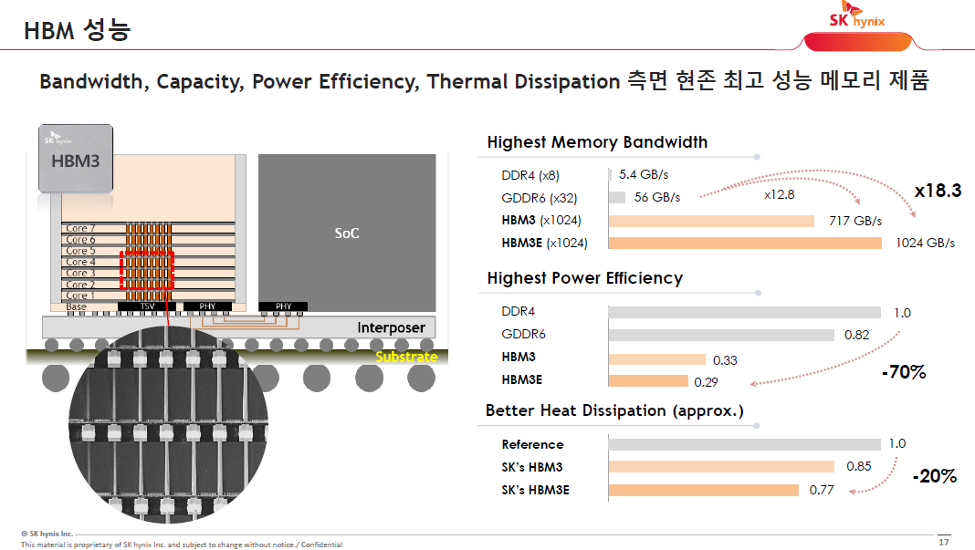
Source: SK Hynix
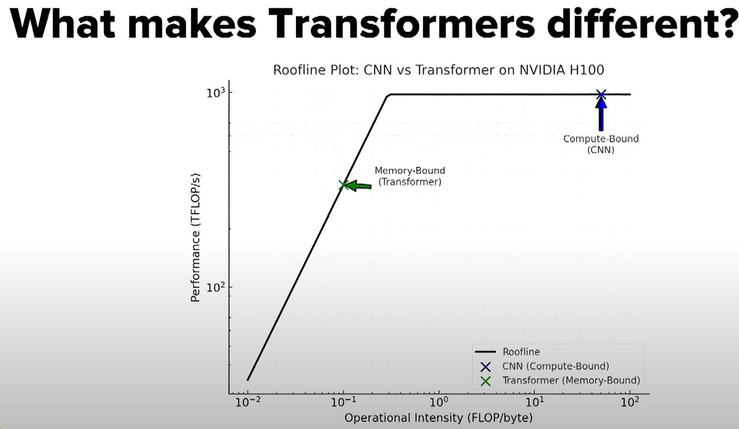
Memory bandwidth is important in the era of Generative AI as model training is often bandwidth constrained rather than compute constrained. The attention mechanism in transformer model has to store and calculate the relationship between all the tokens. Memory requirement is quadratic in proportion to the sequence length. Similarly, memory is also a bigger constraint during inference, due to the need to handle longer context windows and enlarged key‑value cache (KV cache) in the transformer model. Memory consumption for KV cache grows linearly with the token size.
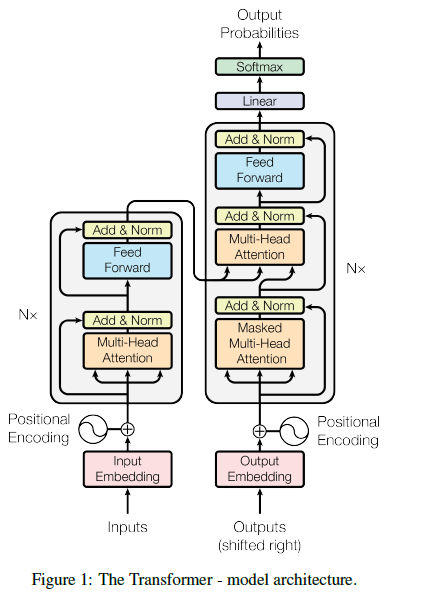
Source: Attention is all you need (2017)
Source: Positron AI
HBM Technology
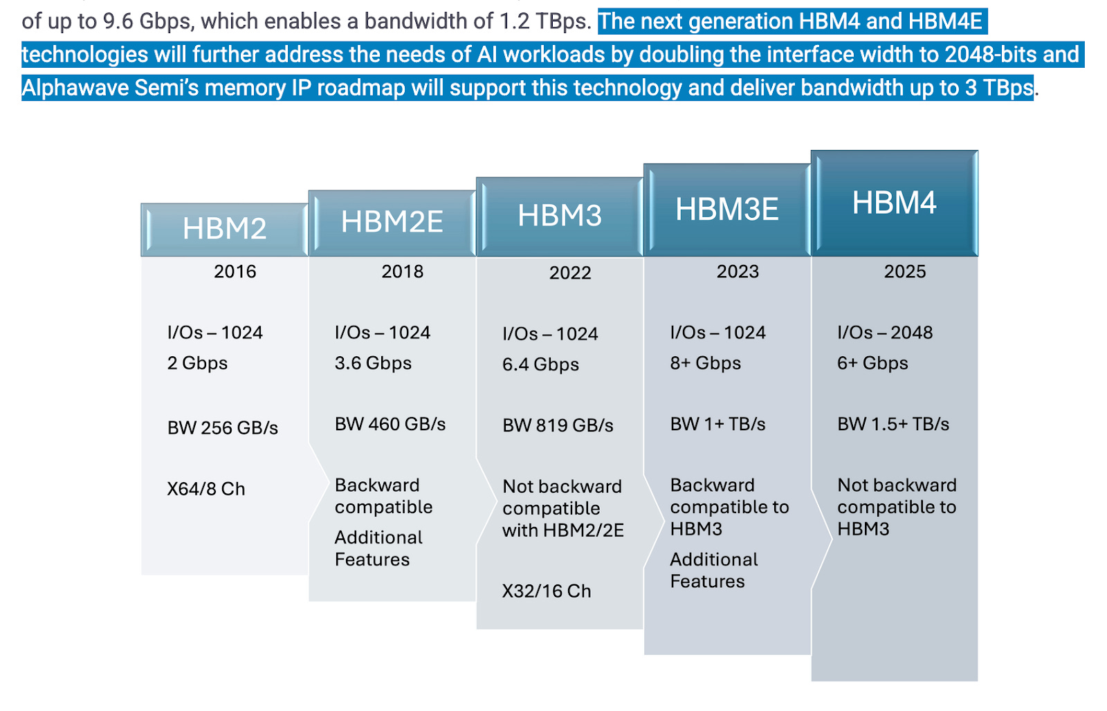
With each generation of AI chip, an upgrade in HBM is a key factor for better performances (higher bandwidth or capacity). In a tick-tock cycle, the main upgrade for NVIDIA GPU in its 2nd generation of the same architecture will be the HBM capacity. 50% jump in HBM capacity from H100 to H200, B200 to B300 and 4x jump from Rubin to Rubin Ultra.
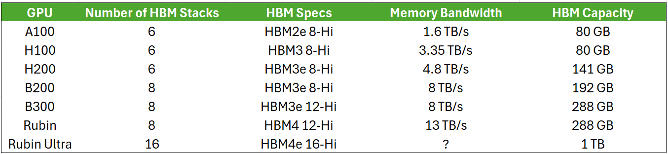
This is in the form of either having more HBM stacks per GPU module, higher number of DRAM dies per HBM module or upgraded HBM generation. HBM4 achieves higher bandwidth by doubling the number of channels per stack from 8 to 16 and a significantly faster I/O per pin.
Source: SK Hynix
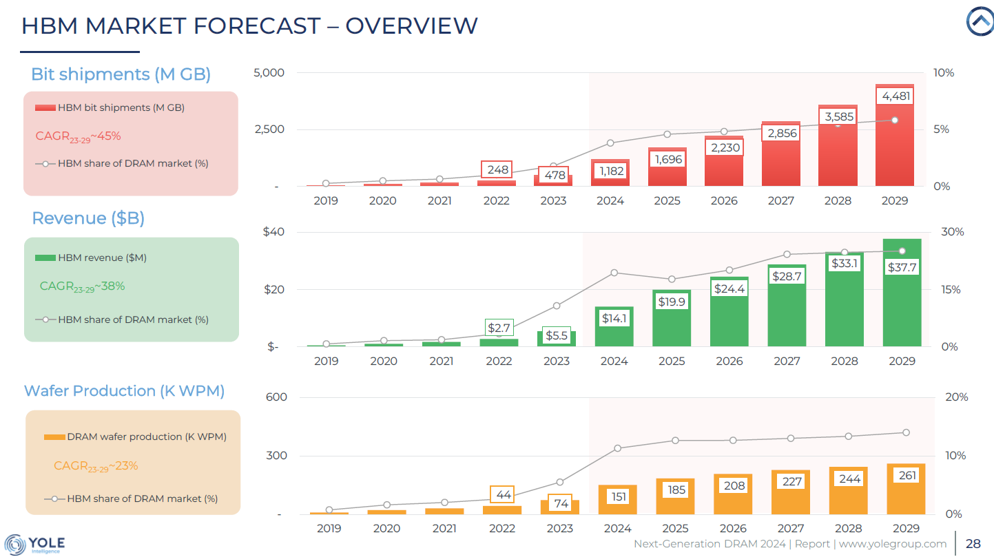
Given the increase in HBM content with GPU and ASICs going forward, the HBM market is expected to grow rapidly. According to SK Hynix, the HBM industry is forecasted to grow at a 50% CAGR from 2024 to 2028. For the DRAM producers, HBM has proven to be less cyclical than traditional DRAM. While volume may still fluctuate in the future, HBM contract pricing is agreed 1 year in advance. This is better than the shorter contract or even spot pricing for DRAM.
Source: Yole
SK Hynix is the current winner of HBM race
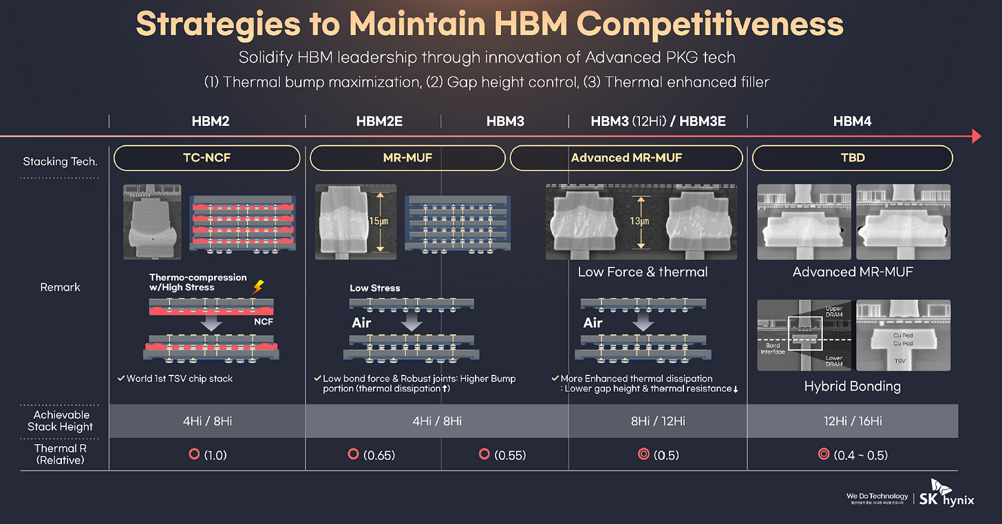
SK Hynix is the winner of the HBM race thus far with its superior MR-MUF (Mass Reflow Molded Underfill) technology. Both Samsung and Micron have chosen the inferior TC-NCF (Thermal Compression with Non-Conductive Film) roadmap. This led to SK Hynix dominating the HBM market with more than 60% market share. This is mainly because SK Hynix serves as Nvidia’s primary HBM supplier for its high end GPU from Hopper to latest Blackwell GPUs (e.g. GB200). Notably, Nvidia accounted for over 60% of global HBM consumption in 2024 and is estimated to account for over 70% in 2025, according to Morgan Stanley.
Source: Samsung Securities
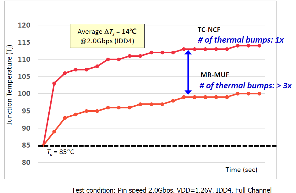
MR-MUF is better than TC-NCF due to better thermal dissipation and higher yield rate. MR-MUF has an average yield rate that is 20% higher than TC-NCF. Thermal dissipation is becoming more important as the number of HBM layers increases over time. More HBM dies stacked together in an area generates more heat. As MR-MUF has 3x the number of thermal bumps than TC-NCF, heat dissipation is much better and HBM can remain at a lower temperature.
Source: SK Hynix
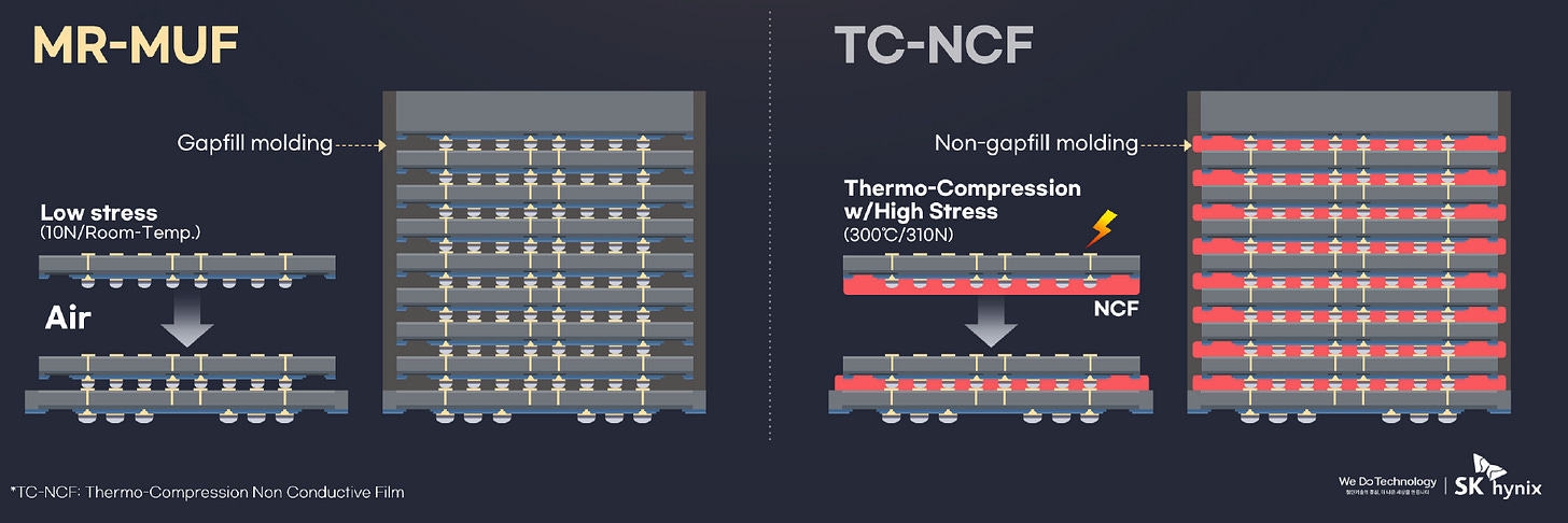
Another feature of MR-MUF is that the process is done at room temperature and with small force, while TC-NCF is done at high temperature of 3000C and strong force. High temperature creates potential warpage issues where the layer will become bent. Strong force also has the potential to damage chips during the stacking process.
Source: SK Hynix
SK Hynix also has an exclusive epoxy molding compound that enables more uniform gap filling and better encapsulation. It reduces voids, enhances heat dissipation and minimizes warpage. The resin-based insulation material is provided through an exclusive contract with a key Japanese supplier called Namics Corporation for many years. This is a key reason why Samsung and Micron are unable to replicate the MR-MUF technology in addition to the patent barrier. With TC-NCF’s film-based underfill, there are tighter alignment tolerances and struggle with flow consistency that gets worse with higher stacks.
Source: SK Hynix
One reason why Samsung has struggled so much is because of their front-end technology. Given that both Samsung and Micron are using TC-NCF, the back-end technology is not the reason why Samsung has yet to be qualified by NVIDIA. Since 1a nm, Samsung had started to struggle with its front-end process. Some attributed it to cultural and management issues, while others said it was due to an aggressive scaling roadmap. Front-end yield rate is particularly important in HBM as the number of HBM dies stacked will continue to grow from 8-Hi to 16-Hi. With a 95% yield rate, the final yield rate will be 66% for 8-Hi and 44% for 16-Hi.
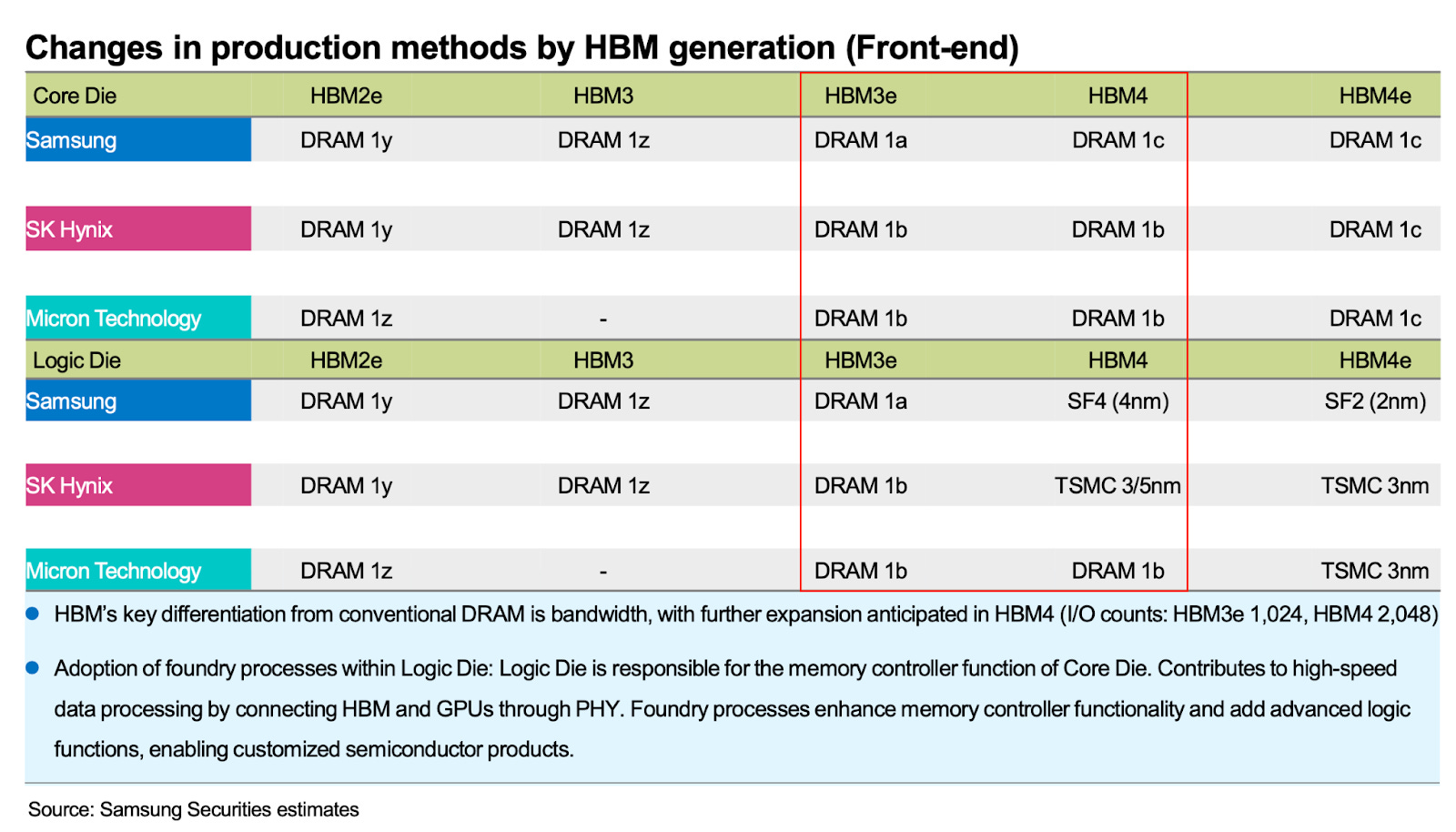
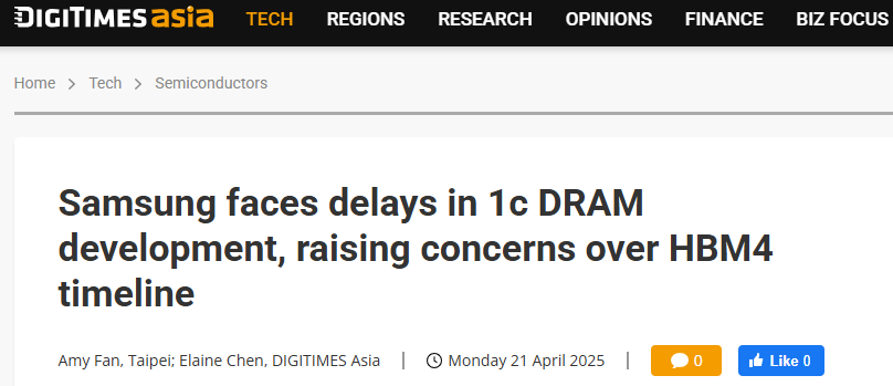
As a result, Samsung is now using 1c nm DRAM die and 4nm logic die for HBM 4 in an attempt to catch up to peers. However, the result for Samsung’s 1c nm is not satisfactory whereas rival SK Hynix had already achieved impressive yield with 1c nm. Note that SK Hynix will be using their mature 1b nm technology for HBM4 given their superior yield rate. Without success at 1c nm development, Samsung is likely to fall further behind in both DRAM and HBM. Unless yield rate at 1c nm can mature in time to more than 90%, it is unlikely for Samsung to catch up to SK Hynix at HBM4. In addition,
Source: Digitimes
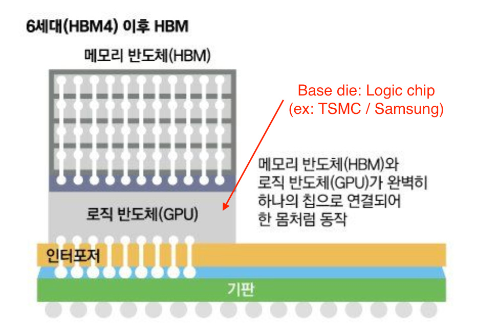
Another key factor should also be factored in the HBM4 race is the migration of the base die from a planar DRAM process to an advanced FinFET logic node.
By moving the base die to logic process technology, it allows the base die to have lower power consumption, boosts transitions performance and gives flexibility for customer-specific features. With FinFET process technology, it turns the base die into a customizable chiplet that provides higher performance with better energy efficiency (especially using more advanced nodes although it's more pricey) while giving memory vendors flexibility to serve hyperscale and accelerator customers for specific purposes.
Source: Joongang Daily
Given such change, Samsung is expected to fabricate this base die in‑house on its own advanced node by reportedly Samsung Foundry’s 4nm process node while industry reports suggest SK Hynix and Micron will outsource theirs to TSMC, likely on 3 nm for customized base die.
The base die for HBM4 essentially has three main functions:
Controlling DRAM Stacks: It serves as the control plane for the entire HBM stack, handling all read/write, refresh, and repair operations across the vertically stacked DRAM layers above it.
Managing the I/O interfaces and Data Transfer: The base die of HBM4 will host 2048‑bit physical layer I/O (JEDEC Standard), which is twice that of HBM3E, and clock network that move data between the memory stack and the host processor in either GPU or ASIC.
Integrating Logic Chips & Customizing HBM4. Since the based die will be fabricated in logic processes (e.g., 4 nm Samsung, 3/12 nm TSMC), it creates room for on‑die power management, ECC (Error‑Correcting Code), and customer‑specific accelerators. With the use of a logic in base die, it also enables “custom HBM” variants and supports advanced 2.5D/3D packaging road maps depending on customer demand for specific workload.
Source: Alphawave Semi
With that in mind, it is clear that the quality of HBM base die are emerging as another key battleground among memory vendors, who increasingly tailor these logic layers to meet customer‑specific power and performance targets for upcoming HBM4. TSMC’s N3 family has demonstrated robust capability and stability over the past three years, so process quality should pose little concern for SK Hynix or Micron.
The key strategic question is whether moving to 3 nm despite its higher wafer cost delivers a tangible performance benefit versus staying on a less advanced node, such as N5 or even N12. Samsung faces a different calculus. Its 4 nm track record remains controversial, and earlier 4 nm-based products have attracted industry criticism. Before HBM4 ramps, Samsung must validate that its in‑house 4 nm process can deliver competitive base‑die quality in comparison to its competitors. If not, it risks falling further behind Micron and SK Hynix, who will leverage TSMC’s proven logic technology, even if Samsung retains a nominal cost advantage by remaining fully integrated.
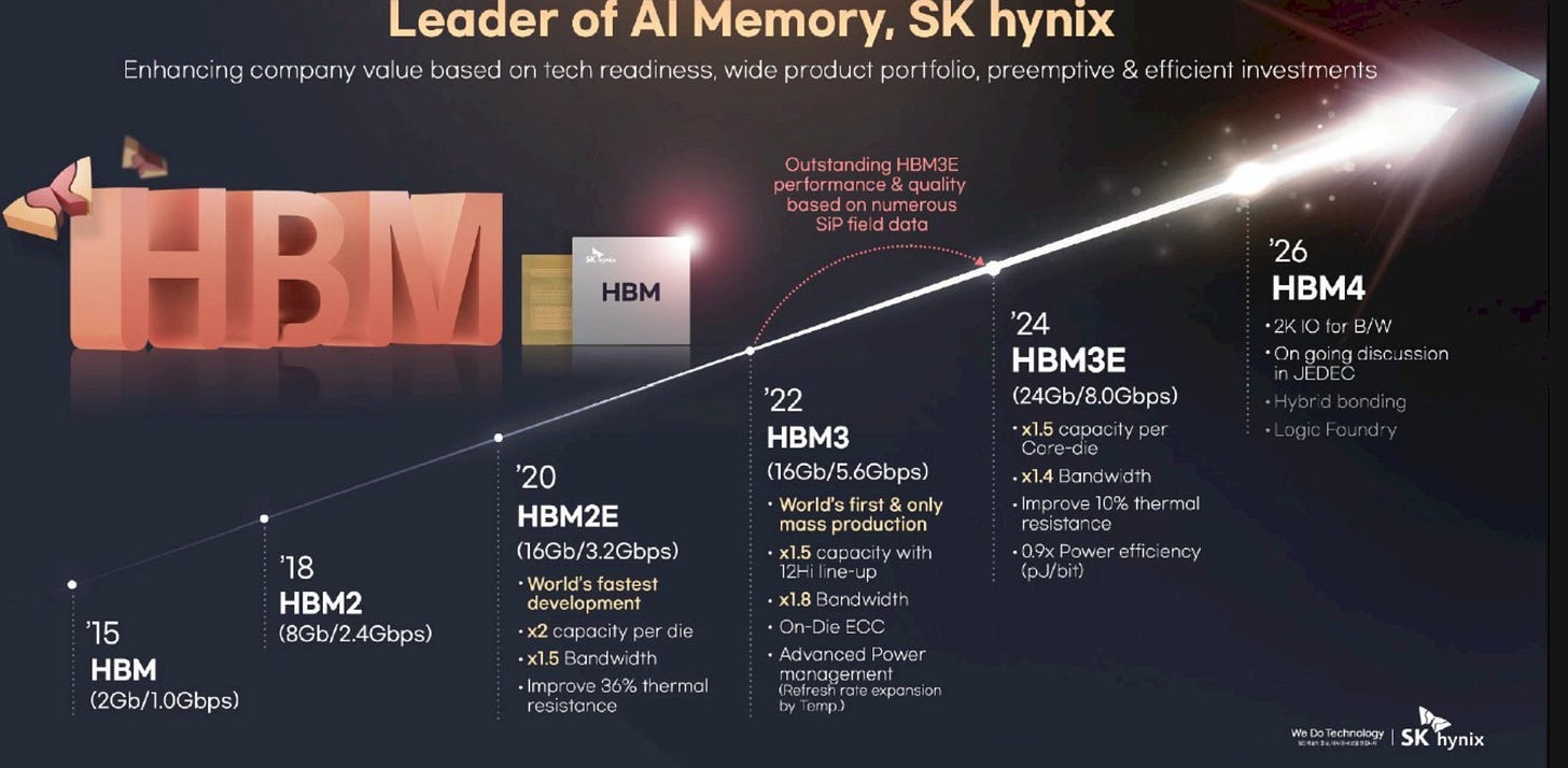
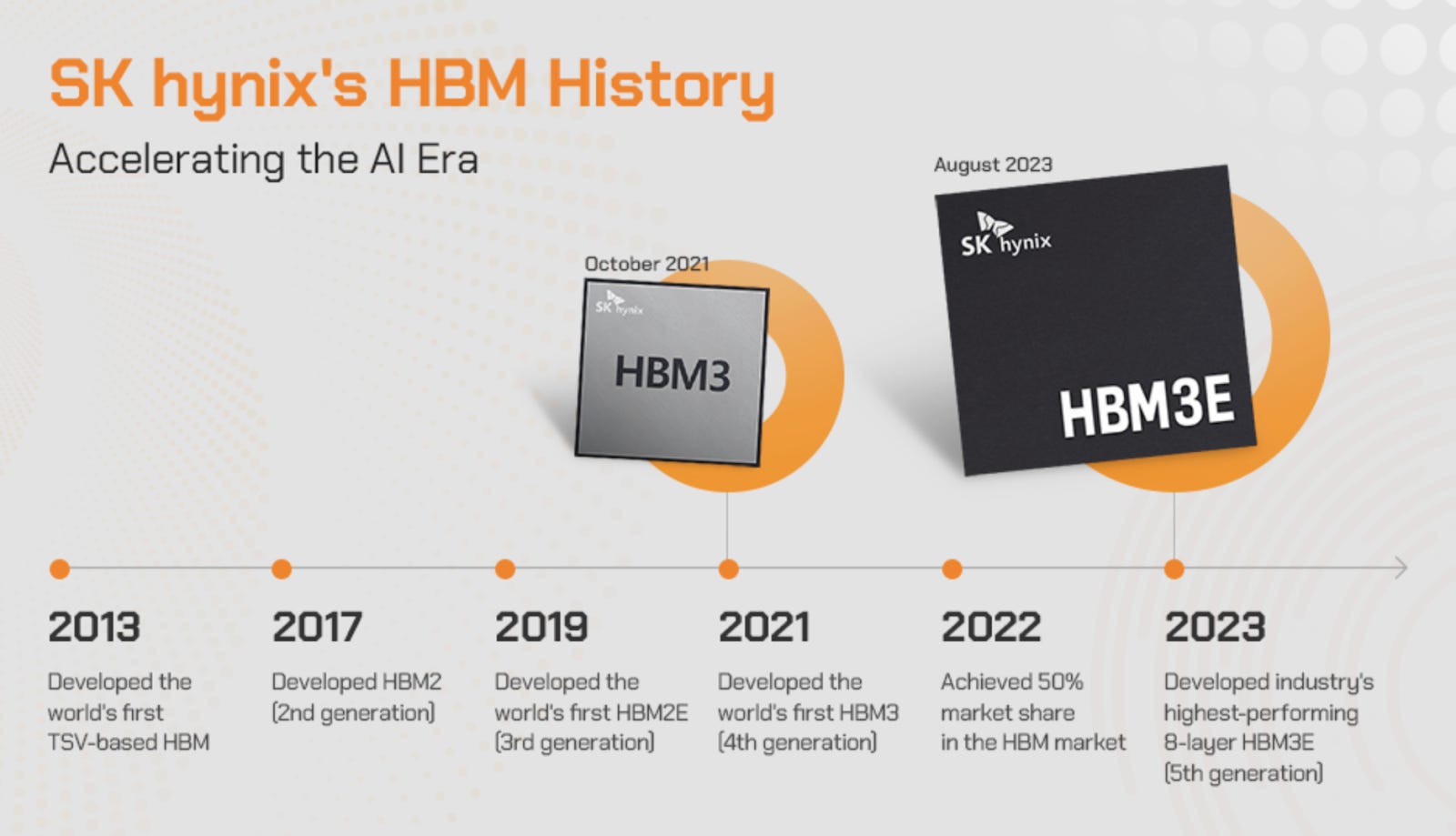
Beyond its superior role in bonding technology and the company's competitive DRAM manufacturing, SK Hynix’s leading role in HBM stems from the company's consistent investment in HBM technology and talent for more than a decade. Since 2013, SK Hynix has consistently invested in HBM technology with its first HBM co-developed with AMD. Early, sustained investment has kept SK Hynix at the forefront of HBM innovation—beginning with HBM2 in 2017, advancing to HBM2E in 2019 and HBM3 in 2021, and culminating in today’s industry‑leading HBM3E and forthcoming HBM4 products.
This first-mover and consistent drive in HBM turned out to be extremely critical for SK Hynix’s success in HBM given the complex manufacturing process required as well as the technical learning curve for the professionals. More importantly, it has enabled the company to continuously identify and align with optimal supply chain partners that match its technology roadmap without disruption.
In contrast to SK Hynix’s steady commitment, Samsung’s engagement with HBM has been rather sporadic. Despite Samsung has kept pace with SK Hynix in HBM in most of 2010s with its first‑generation HBM and HBM2, the firm decided to dismantle its HBM team in 2019, citing the limited market potential of HBM. This was a move that likely stalled technical progress and, more damagingly, severed the talent pipeline needed for future HBM development in coming years. In hindsight, the decision is clearly a significant strategic misstep by Samsung.
More importantly, the timing is proven fatal as the team was dissolved only about three years before the AI boom driven by launch of ChatGPT-3, which is the key period of time for companies to gear up developing the key HBM to power the AI chips, such as HBM3 and HBM3E, which later powered Nvidia’s most popular and widely adopted H100.
Samsung’s strategic retreat from HBM also coincided with SK Hynix’s technological breakthrough in HBM. It was exactly in 2019 when SK Hynix unveiled its MR-MUF bonding technologies, as previously noted, the key technology that helped the firm's HBM products stand out from the competition with Micron and Samsung.
Source: SK Hynix
Hybrid Bonding is a game-changer for HBM
As a result of the superior MR-MUF technology, SK Hynix has dominated the HBM market. However, the leadership position is susceptible to change if hybrid bonding is adopted for HBM. As hybrid bonding is a new technology, whichever player first mastered it will have an advantage in the learning curve.
In hybrid bonding for HBM, the process begins with surface preparation of the die to be bonded, creating planarized copper pads and surrounding dielectric layers. These surfaces are then chemically treated and activated to ensure high-quality adhesion. Next, the dies are precisely aligned and directly bonded to form both a copper-to-copper connection and a dielectric-to-dielectric mechanical bond. Once bonded, the stack undergoes low-temperature annealing (typically <400°C) to strengthen the interconnects.

Source: IEEE Spectrum
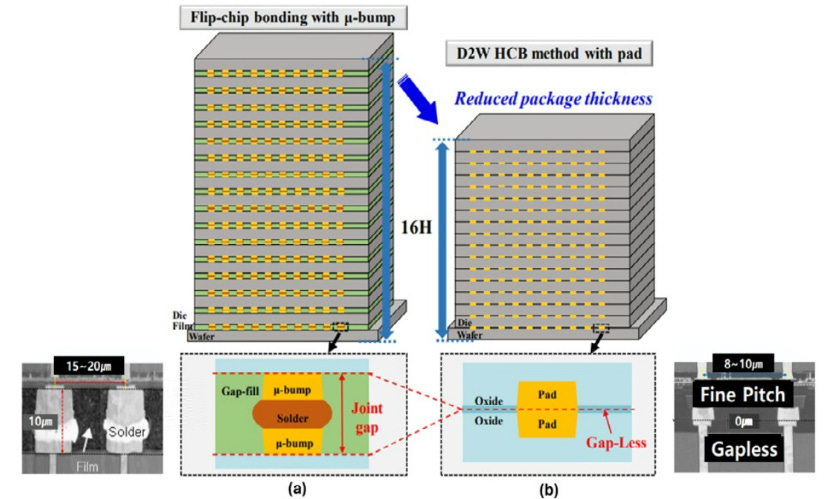
Hybrid bonding enables direct Cu-to-Cu (copper-to-copper) bonding between stacked dies without the use of micro-bump. This solution offers much tighter pitch, lower resistance and better thermal characteristics. Hybrid bonding supports below 10μm pitch (vs ~40-55μm for microbumps), allowing many more connections between layers. With a tighter bump pitch and no gap between HBM dies, the overall stack height of HBM can also be reduced.
Source: Samsung
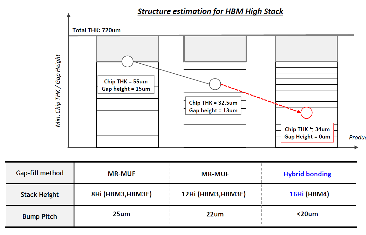
Initially, JEDEC had specified a package height of 720um for HBM. This was possible to achieve for both 8-Hi and 12-Hi HBM3/3E using both MR-MUF and TC-NCF. As we move to 16-Hi HBM4, hybrid bonding was supposed to be an inevitable technology requirement to meet the 720um height. With some lobbying, JEDEC relaxed the package height to 775um for HBM4. This allows the usage of both MR-MUF and TC-NCF for HBM4. Other than reducing overall stack height, hybrid bonding improves overall power and bandwidth through higher density and shorter connection between the dies.
Source: SK Hynix
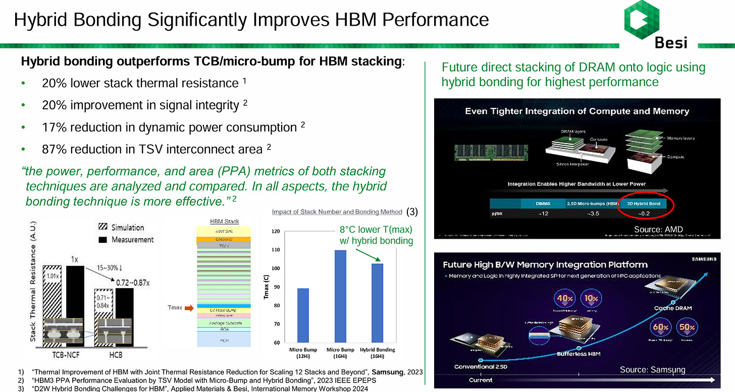
Source: Besi
The main reason why hybrid bonding is not yet adopted for HBM is that it costs a lot more than the current method. Hybrid bonder costs USD 3 million as compared to USD 1-2 million for TCB.
In addition, the total cost of ownership is much higher due to additional CMP (Chemical Mechanical Planarization) steps and the requirement for higher-class cleanrooms. CMP is needed to ensure both dies are smooth and flat at the bonding interface. As a result of the cleanroom requirement, other tools such as grinder, dicer and die placement will become more expensive as they have to meet front-end specifications. Hybrid bonding is also where the line of front-end and back-end gets a little blur.
While Samsung and Micron will try to get ahead of SK Hynix with hybrid bonding, the timeline for hybrid bonding mass adoption is likely to be in 2028 or 2029 for HBM5 20-Hi. This is also in line with NVIDIA’s roadmap where we will see HBM5 adoption only in late 2028 at the earliest to be paired with the next generation of GPU after Rubin Ultra.
We can also deduce from the volume production date of the 2 new advanced packaging facilities that Micron and SK Hynix had invested in. Micron broke ground on a $7 billion HBM advanced packaging facility in Singapore in 2025 with mass production expected in 2027. SK Hynix plans to invest $3.87 billion in their new Indiana advanced packaging plant which will start production in 2028.
Source: SK Hynix
HBM Equipment Suppliers
There are a few key equipment suppliers for the HBM market
Thermal Compression Bonder (TCB): Hanmi, Hanwha, ASMPT, Kulicke & Soffa, Semes
C2W Hybrid Bonder: Besi, ASMPT, SUSS Microtec
Metrology: Camtek, KLA
Molding: ASMPT, Besi, Towa
Grinder: Disco
CMP: Applied Materials, Ebara
Temporary Bonder, Debonder: SUSS Microtec, Tokyo Electron
Tester: Advantest, Teradyne
TSV: Applied Material, LAM Research, Tokyo Electron
Within the supply chain, TCB and Hybrid Bonder receive the most attention due to the intense competition landscape. Bonder tools are also required to stack the HBM dies on top of each other.
TCB is currently the mainstream bonder equipment used by SK Hynix, Samsung and Micron. TCB market for HBM packaging is currently led by Korean firms like Hanmi Semiconductor and Hanwha Precision, both of which supply to major DRAM makers like SK Hynix and Micron. Hanmi is especially dominant in HBM3 and HBM3E with its superior cost-performance and productivity. The company has been the top supplier for SK Hynix till today despite some of the disputes that they have. Hanmi is also the main supplier of TCB to Micron and the Chinese producers.
While ASMPT and KLIC (Kulicke & Soffa) are also active in the TCB market, their historical strength has been more on logic packaging. Precision level is higher in logic than HBM packaging, which justifies the higher cost of their machines.
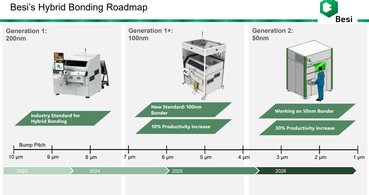
The C2W (Chip-to-Wafer) hybrid bonder market for HBM is still in its early stages but rapidly becoming a key battleground. The industry is transitioning from microbump-based TCB to bump-less Cu-to-Cu hybrid bonding for HBM5 and beyond. While TCB vendors may attempt to evolve into hybrid bonding, they require partnership with front-end equipment producers. To this end, Besi has partnered with Applied Materials and ASMPT has partnered with EV Group. Applied Materials have contributed their expertise in etching, CMP, deposition, cleaning, metrology and inspection to the partnership. For those who are not familiar with EV Group, this company is the undisputed market leader in Wafer-to-Wafer permanent bonder. Korean vendors such as Hanmi and Hanwha are also exploring hybrid bonding extensions of their TCB platforms, but they currently lack the precision and low-temperature process control.
Currently, Besi is leading in the hybrid bonder race with the current 100nm accuracy hybrid bonder and upcoming launch of Generation 2 50nm precision hybrid bonder that achieves bump pitch of <4 um. For both ASMPT and KLIC, they are trying to delay the adoption of hybrid bonder with their next generation fluxless TCB tool (AOR TCB by ASMPT, APTURA™ FTC by KLIC) that allows placement accuracy of sub-1 um and <10um bump pitch.
Source: Besi
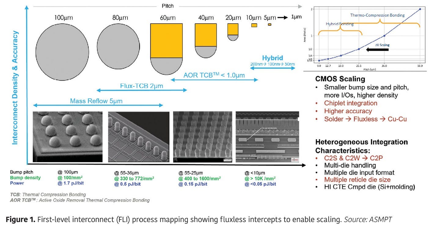
Source: ASMPT (AOR TCB)
China’s Catch Up in HBM
China’s progress in HBM remains limited in comparison to three top memory makers and poses little immediate concern for them, especially when the memory development in China is under the shackle of the U.S.-led restrictions on semiconductor manufacturing equipment, including lithography, etching, TSV, and etc. However, China has a proven track record of rapidly advancing its memory technologies despite regulatory challenges, as demonstrated by two leading memory makers CXMT and YMTC in recent years.
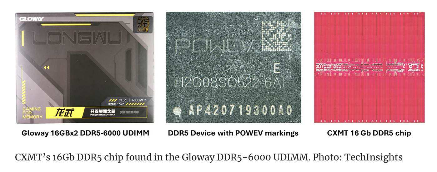
In particular, CXMT, founded in 2016, has been the DRAM leader in China and has advanced rapidly in the traditional DRAM area over the past few years, challenging the three memory giants marketplace in mid to low-end DRAM (e.g. DDR3 and DDR4). Besides, the company has quietly moved into rather advanced DRAM DDR5 earlier this year, narrowing the gap with DRAM leaders.
Source: TechInsights
CXMT’s progress in HBM has been relatively slow. Prior to the surge in high-performance computing demand that began in late 2022, the company had not prioritized HBM technology, causing the company to fall behind the HBM development. Another reason, clearly, is the company's lagging development in DRAM, which underpins the front-end manufacturing for HBM.
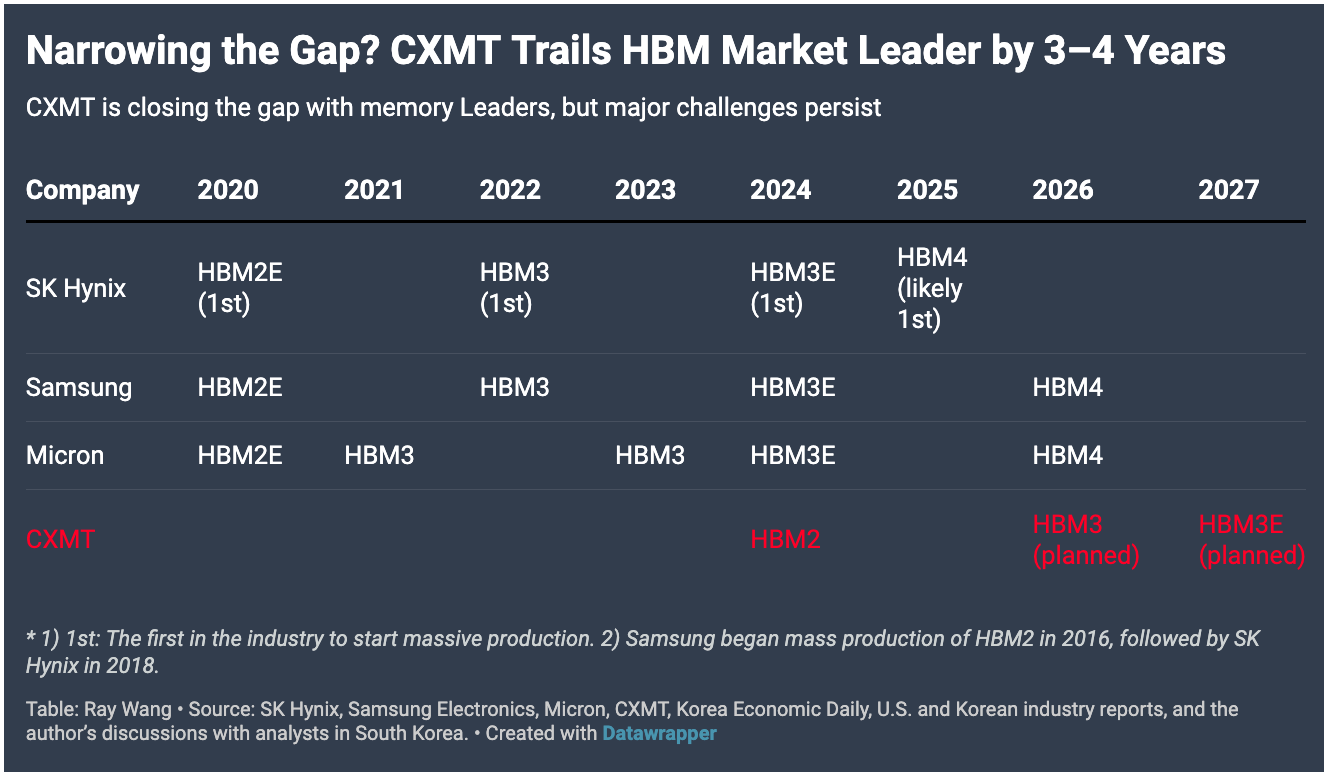
Yet, CXMT is seeking to catch up with the HBM technology. In the second half of 2024, CXMT reportedly began mass production of HBM2. However, adoption of CXMT’s HBM is expected to remain at best, elusive, within China for now, given the availability of more advanced HBM products from SK Hynix and Samsung prior to restrictions, as well as the fact that local customers are unlikely to adopt the much less advanced products from CXMT. Moreover, CXMT has so far had only small volume production and shipment for its HBM products.
Currently, CXMT is working on HBM3 and planning for mass production in the following year. This should narrow the gap between CXMT and HBM leaders to about four years. Moreover, the firm aims to announce HBM3E and push for mass production in 2027; a quite ambitious roadmap given firm’s relatively immature DRAM and HBM technology.
Source: Ray Wang
Analysts attending this year’s SEMICON China, which took place in Shanghai, noted that they expect the rapid advancement in HBM through 2025, noting that HBM3E is the primary target specification for domestic HBM firms. While this does not indicate that China is on the verge of successfully developing HBM3E, the fact that domestic firms are actively developing around this specification implies meaningful progress in Chinese HBM technologies. At a minimum, it signals that China’s memory industry is working on the most cutting-edge HBM.
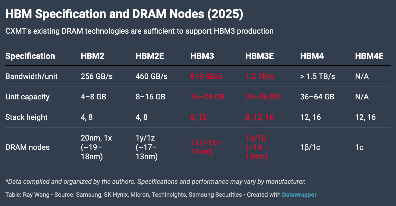
Looking through a more technical lens, CXMT appears increasingly capable of producing the DRAM die for both HBM2E and HBM3, building on its progress in DRAM. The company is currently able to manufacture DRAM at the 1y nm and 1z nm nodes used in these two generations of HBM. Another leading technology consultancy, TechInsights, confirmed in its January analysis that CXMT is capable of manufacturing DDR5 at the 1z nm The density of CXMT’s DDR5 is comparable to that of leading global competitors (Micron, Samsung, and SK Hynix) in 2021 though the chip exhibits a larger die size and an unverified yield rate.
CXMT’s R&D team is likely developing sub-15 nm DRAM nodes, specifically the 1α nm, which are essential DRAM nodes for HBM3E. Although CXMT will likely face major challenges in developing 1α nm without Extreme Ultraviolet Lithography (EUV), it is not impossible to develop 1α nm without EUV. In 2021, Micron debuted its 1α nm DRAM without the use of EUV, paving a potential track for CXMT to duplicate.
Source: Ray Wang
On the back-end process, for now, CXMT is likely to use TC-NCF bonding technology for its HBM product, given the company has similar access to most semiconductor manufacturing equipment (besides EUV) essential for HBM as other memory makers like Sasmsung and Micron prior to the December 2024 export controls. Even after the export controls, Hanmi Semiconductor continues to be the key supplier of TCB for various Chinese customers, which likely include CXMT, Tongfu Microelectronics, and other key players in China’s HBM space. Until very recently, Hanmi Semiconductor reportedly halted shipment of TC bonders to Chinese customers, likely due to the pressure from the U.S. government.
Taken together, CXMT’s capability in front-end and back-end technology in HBM will be key to watch regarding the future advancement for its HBM product, including HBM3E. In particular, the maturity of its front-end technology, namely D1z and D1a, will likely define the success of its forthcoming HBM product as its TC-NCF bonding should yet to be a problem to bite given firm’s stockpiled bonding equipment from South Korean equipment providers.
Given that CXMT has recently begun mass production of DDR5 using its 1z nm, yield issues with D1z are likely becoming less of a concern for its future HBM3 development although it will still take time for the firm to further improve yield and product quality. However, as the company aggressively pushes forward its front-end roadmap, it is expected to face significant challenges with the D1a node particularly in achieving competitive yield and scaling due to the absence of EUV lithography. As such, as of now, it is reasonable to believe CXMT is about 3 to 4 years behind leading memory makers in terms of HBM3 and HBM3E.
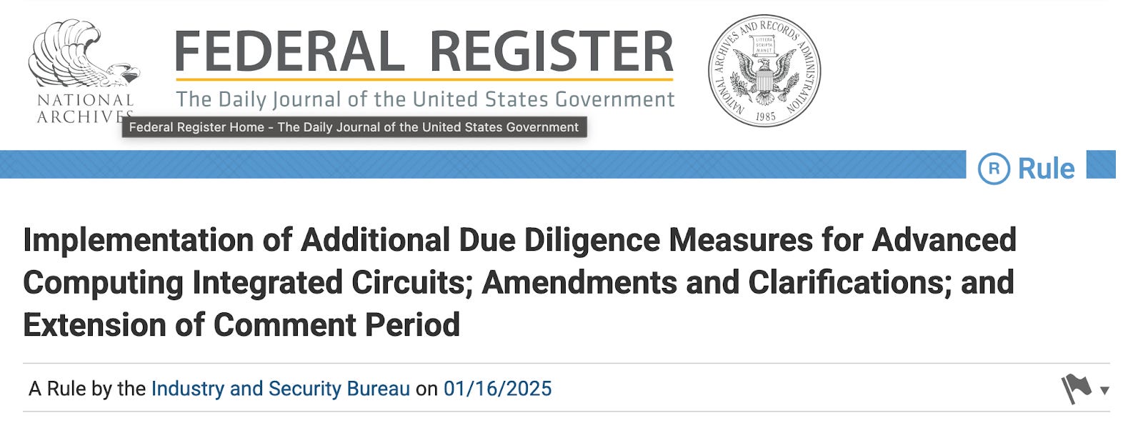
Source: Federal Register
In January 2025, BIS further tightened the definition of advanced node IC for DRAM to
A memory cell area of less than 0.0026 µm2;
A memory density greater than 0.20 gigabits per square millimeter; or
More than 3000 through-silicon vias per die. (*Samsung’s HBM2 has > 5000 TSVs per die and SK Hynix’s HBM3 > 8000 TSVs per die)
The stricter rule could restrict CXMT’s ability to expand beyond 18nm as the October 2022 rule had allowed CXMT to pursue up to 1z nm despite the headline restriction at 18nm.
Looking ahead, besides paying attention to China’s front-end technology in HBM, it is important to closely monitor Chinese companies’ pursuit and potential adoption of hybrid bonding in their future HBM technologies. As previously emphasized, hybrid bonding could represent a pivotal turning point that reshapes the competitive landscape of the HBM industry. For the Chinese memory industry, hybrid bonding may offer a pathway to significantly accelerate their HBM development, perhaps not to surpass global leaders, but to more meaningfully narrow the gap.
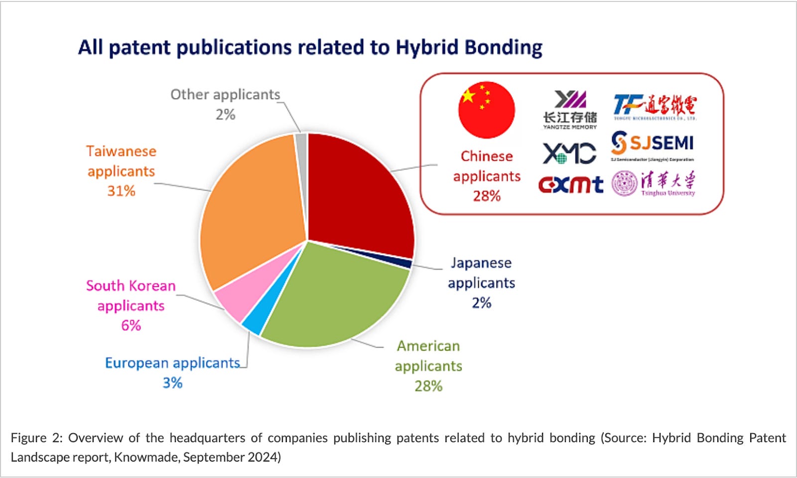
Source: Knowmade
Clearly, Chinese companies are aware of hybrid bonding’s importance to HBM. Key HBM players such as CXMT and Tongfu Microelectronics have been investing in the research on hybrid bonding in recent years, with reports indicating a notable acceleration in their patent filings related to the technology since 2022 when China’s semiconductor industry faced increased U.S. restrictions.
Leadership in next-generation HBM will increasingly depend not only on a company's front-end DRAM manufacturing capabilities but also on its ability to be first to master and integrate hybrid bonding into its HBM products, setting itself apart from competitors. This should be the case for South Korean, U.S., and Chinese memory players.
 | A guest post by
|
Outstanding summary of the package options. Thanks.
Really insightful post. thank you! can I ask - does the memory bandidth bottleneck fall away outside of training i.e. when doing Inference - is bandwith less of an issue?