
The nature of Moore's Law
Why the industry always gets bigger over time

Moore’s Law is the observation made by Gordon Moore in 1965 that the number of transistors doubles every years. This was subsequently revised to a doubling in the number of transistors every 2 years. The exponential increase in transistors has been a key driver of numerous innovations over the many decades.

Source: Wikipedia
Moore’s Law as a business model
While there have been numerous concerns over the death of Moore’s Law, this is a misconception of its nature. If Moore’s Law is a scientific law, Gordon Moore will not have changed his prediction on the cadence of Moore’s Law.
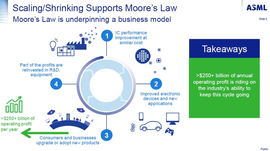
Best explained by ASML, Moore’s Law is in fact a business model of the semiconductor industry. The continuous improvement in transistors cost drives improvement in performance, power consumption and cost of the end devices. We have gone from mainframe to PC, smartphone and now AI. These new and better devices enlarge TAM for the semiconductor industry with a part of the profit reinvested in R&D to continue the Moore’s Law.
This is a business model that shares the value creation from Moore’s Law between equipment vendors, foundries, fabless, EDA, OEMs and end consumers. As a business model, Moore’s Law will continue to drive improvement in end devices for numerous decades ahead.
Source: ASML
Moore’s Law puts the incumbent and market leader in a very dominant position if they do not give up on the business model. Even when Intel succeeds in achieving 5 nodes in 4 years, they are still behind TSMC in 2026 as TSMC has moved to N2 node. It is always for the leader of Moore’s Law to lose their lead, not for the followers to catch up. This was exactly what happened to Intel from 2014 until TSMC achieved node parity in 2019 with N7.
As the industry strives to achieve improvement in PPAC (performance, power, area, cost), there are constant innovations taking place. The ecosystem is such that the leaders in the different parts of the value chain are incentivized to work with each other as much as they wish to capture a bigger part of the profit pool for themselves. TSMC will not entrust their proprietary process technology to an EDA startup. Front-end equipment vendors have access to the future roadmap of their foundries and IDM customers. This is the ecosystem moat that leaders in the semiconductor industry benefit from, allowing them to deliver positive economic returns on capital.
Where will Moore’s Law go from here?
Moore’s Law has slowed in recent years as we approach physical limitations. However, there is still a good visibility in the direction of roadmap extension. For logic, transistor scaling will increasingly be 3D since we entered FinFET era. In 2025, TSMC will start mass production of N2 with the Gate-All-Around (GAA) nanosheet architecture. Backside Power Delivery will also be introduced at Intel 20A in 2024 and TSMC A16 in 2026. High-NA EUV ecosystem could be ready after 2028. Beyond that, IMEC has a roadmap through forksheet and CFET.
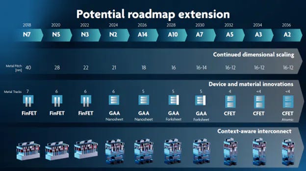
Source: IMEC
In memory, NAND producers have been able to rely on 3D NAND to drive annual density growth of more than 30%. Instead of shrinking NAND cell, bit density growth is achieved through stacking more layers of cells on top of one another. Today, Samsung is delivering 236 layers V8 NAND and has roadmap for NAND with up to 1000 layers. The high number of layers stacked leads to demand for high aspect ratio etching tool. This is currently dominated by Lam Research, while Tokyo Electron is winning POR for its cryogenic etching tool for 400L NAND. 3D NAND migration will continue to lower cost of NAND and help to improve the economics of SSD against HDD. However, this reduces the potential for NAND industry to further consolidate as scaling is easier than in DRAM and logic.

Source: Samsung
For DRAM, EUV insertion will be the key as they migrate beyond 1z nm. Samsung and Hynix are moving on to 1c nm which will have 6 to 8 layers of EUV. Micron will be introducing EUV to its 1-gamma node in 2025. DRAM producers will gradually increase the number of EUV layers before High-NA EUV is used. 3D DRAM will arrive in the next decade, although 3D DRAM is very different from 3D NAND.
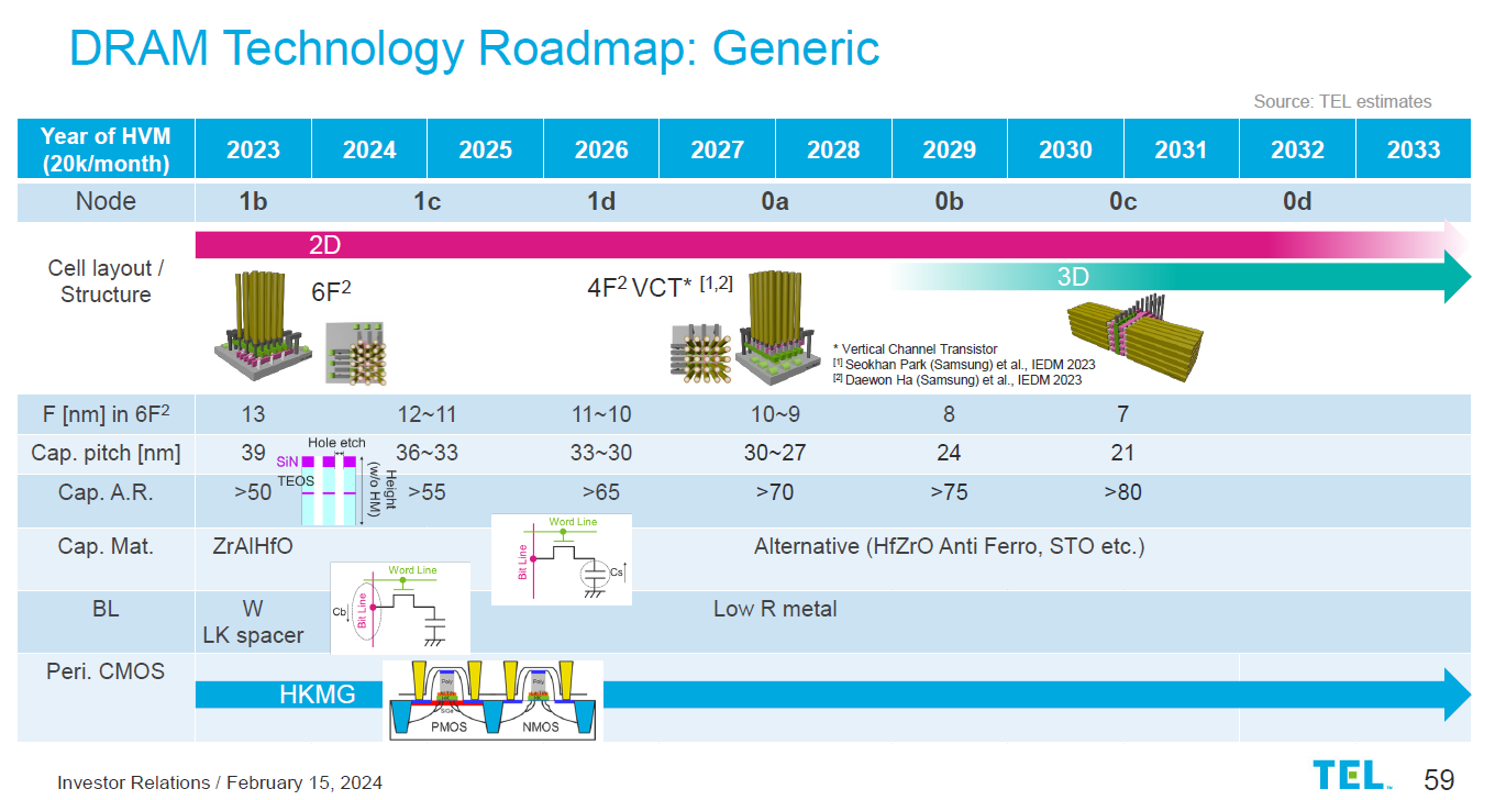
Source: Tokyo Electron
More than Moore’s Law
Advanced packaging is becoming more important as traditional shrinking of transistors is getting more complex and costly. Chiplet is a solution as die size is approaching reticle limit. Power consumption can also be reduced by putting DRAM and logic die closer to each other.
TSMC has been a leader in advanced packaging with more than a decade of investment in 2.5D (Chip on Wafer on Substrate, CoWoS) and 3D packaging (System on IC, 3D SoIC). Apple is one of the early adopters of TSMC’s InFO (Integrated Fan-Out) for its mobile SoC. Intel has also introduced its EMIB (Embedded Multi-die Interconnect Bridge) and Foveros process.
HBM (High Bandwidth Memory) has gained prominence in this current AI upcycle. Through stacking 8 to 16 DRAM dies vertically and connected TSV (through silicon via), much higher bandwidth can be achieved in the packaged module. TSMC’s CoWoS-S process connects the HBM and GPU dies through the silicon interposer for Nvidia’s H100. Nvidia’s next generation B100 will utilise TSMC’s CoWoS-L which can support bigger package size through the use of redistribution layer.

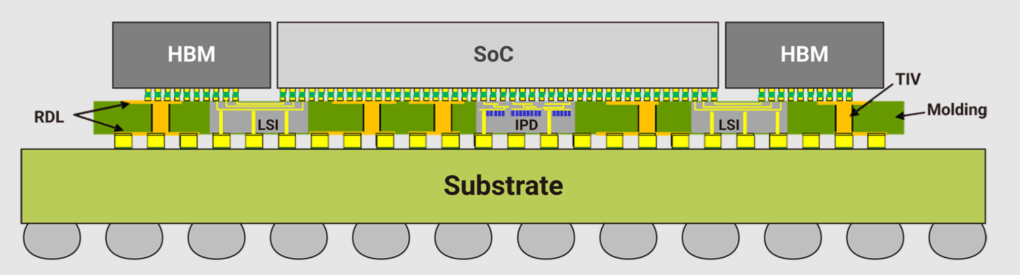
Source: TSMC
Hybrid bonding, which will allow <10um pitch size, is the direction for both logic and memory. Despite the recent relaxation of HBM height limit by JEDEC, hybrid bonding will eventually be adopted for HBM5. For logic, TSMC’s SoIC will see more customers adoption and Intel will be using it for Foveros Direct.
Conclusion
While Moore’s Law no longer works the way that Gordon Moore has observed 6 decades ago, the business model that underpins the semiconductor industry is well alive. Equipment vendors that are enablers of Moore’s Law benefit through higher market share and higher margin products. Leading foundries and IDMs are incentivised to be the leader of process technology, else they risk losing their high returns.